I’m moving to a different country for an unspecified length of time, and have
made the difficult decision to leave my behemoth of a desktop PC behind.
Initially I was planning on just living off of my Framework 12th gen laptop,
which is a very capable little machine, but then managed to convince myself
that it would be fun to build a small form factor desktop that it would be
practical to ship to the other side of the world. My design goals in
researching cases were:
Must be small enough to easily ship internationally, but large enough to fit
a performance CPU and a cooler that is at least ‘adequate’
Does not have to have enough space for a GPU, but it’s a bonus
Would ideally be pleasing to look at as a desk object, since storage space
will be at a premium in my new location.
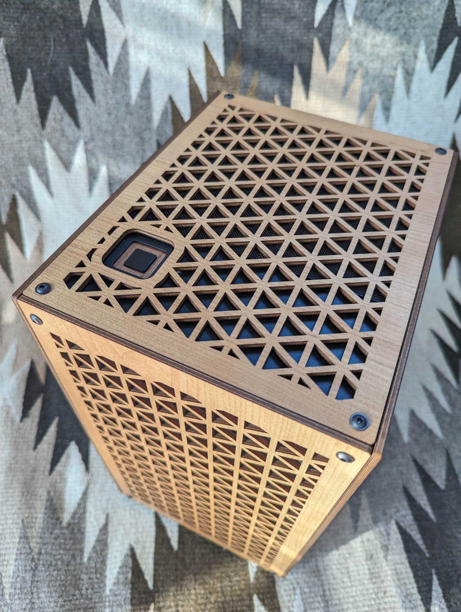
After looking around, I ended up settling on the
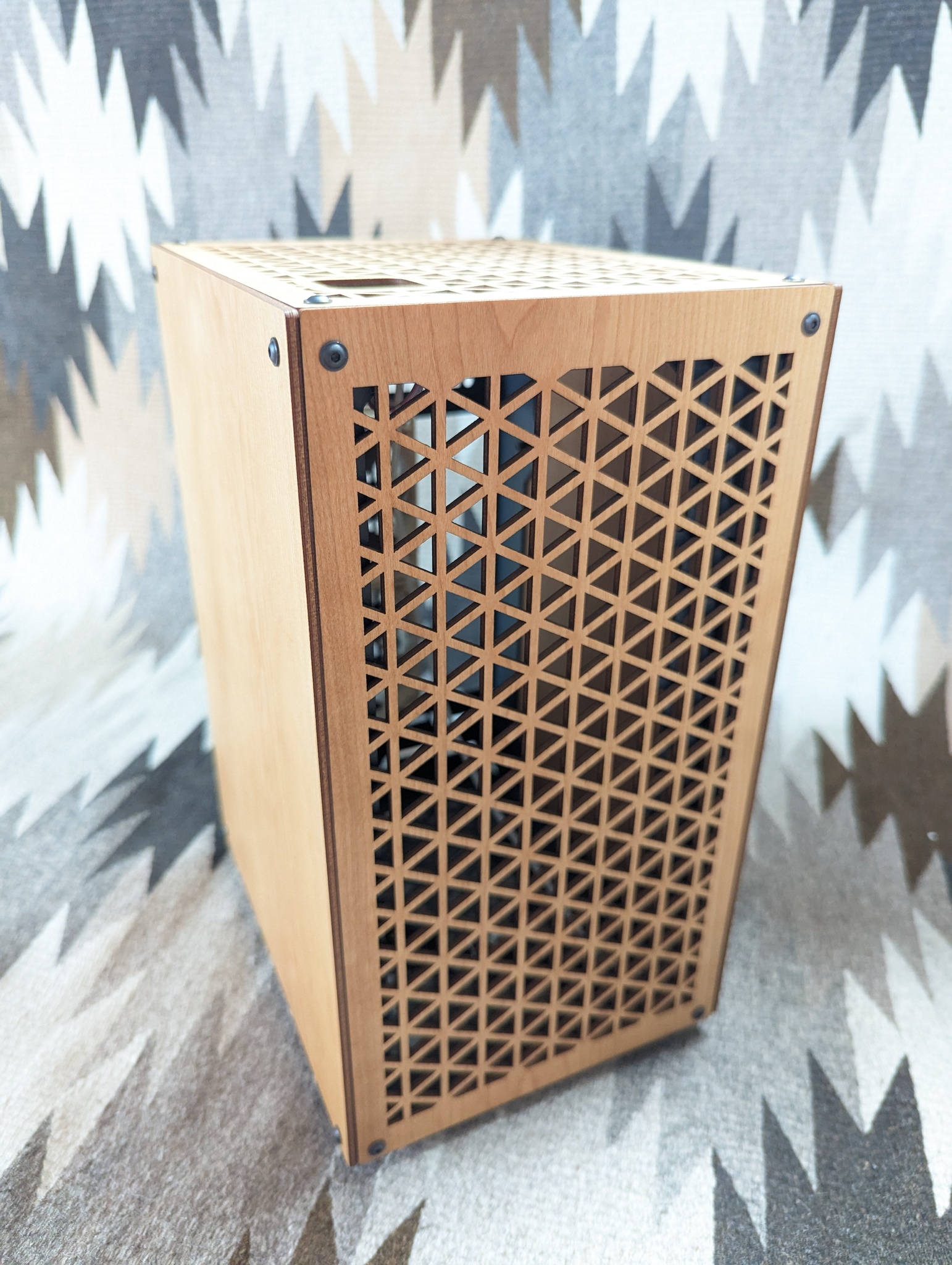
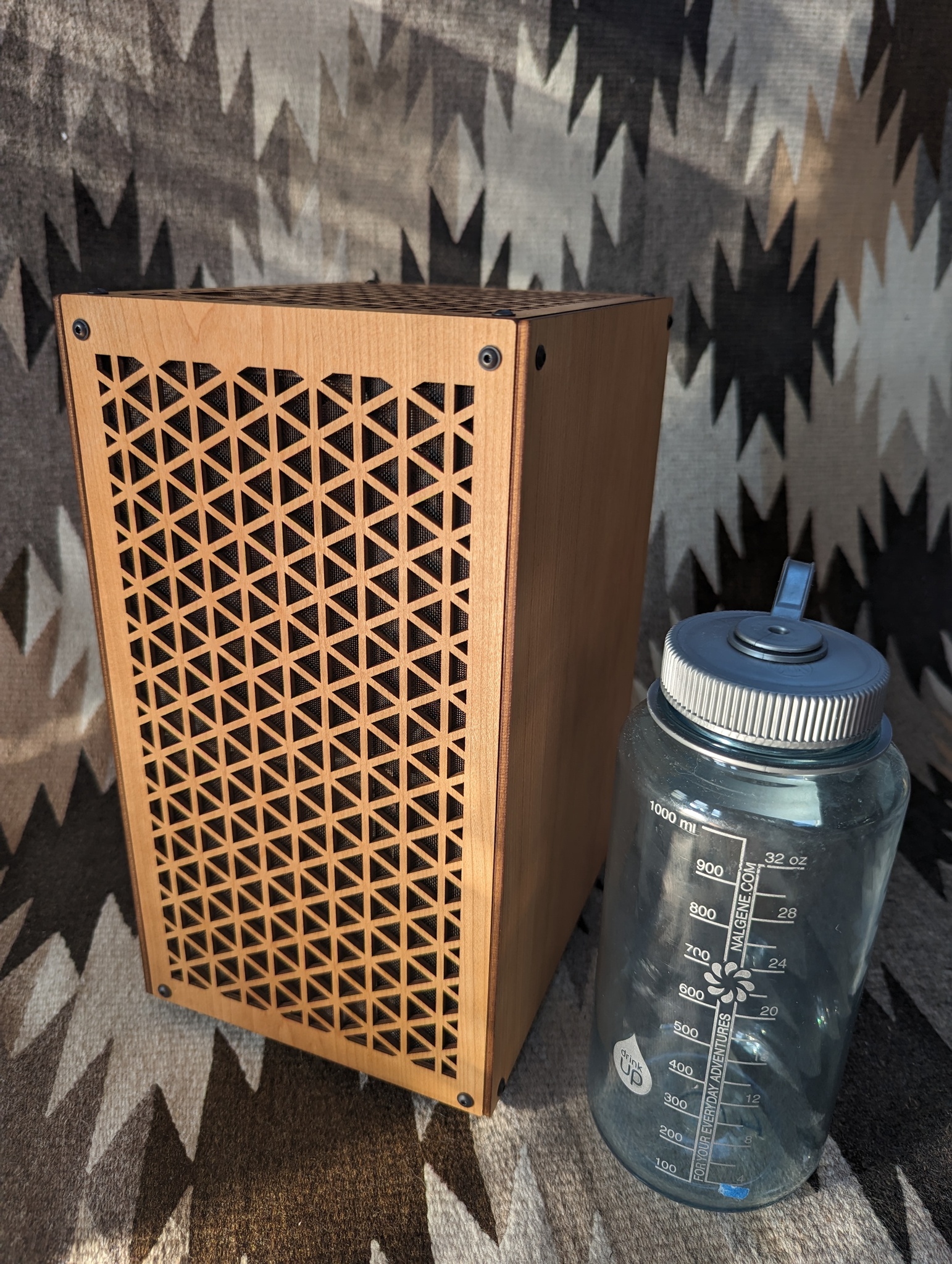
Cubeor Aski 2,
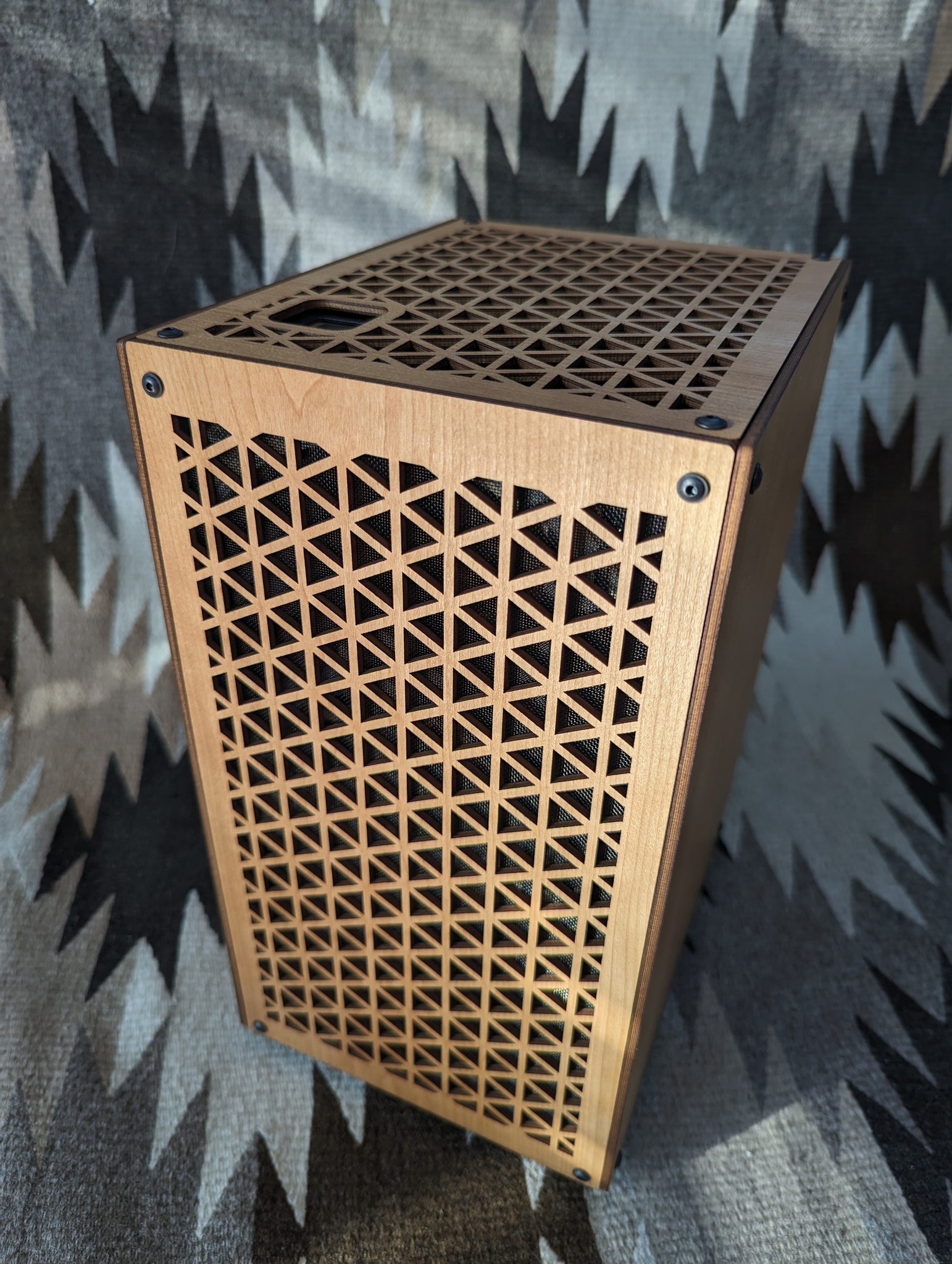
a 10L small form factor computer with fetching laser-cut wood panels. Key
features that seemed attractive are the space for a large number of fans (to
help cool a performance CPU), the ability to insert a GPU without a riser
(simpler build process) and aesthetics (I love the wood panelling). After
ordering the case, I then specced out the internals as follows:
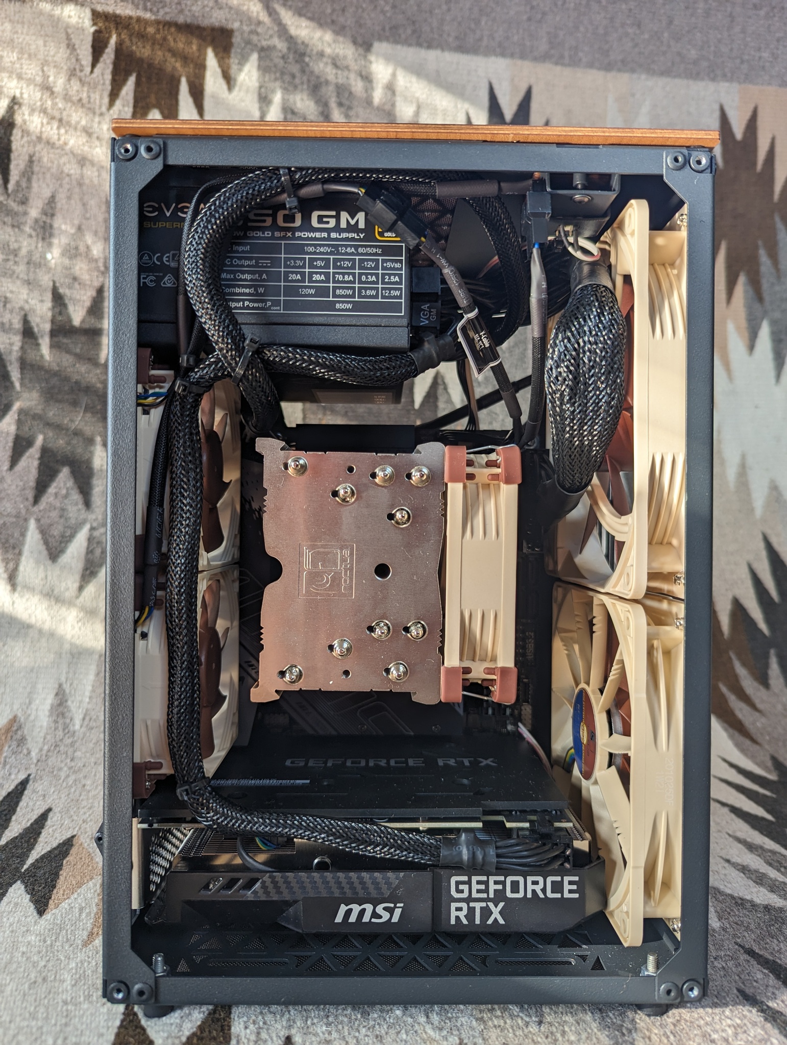
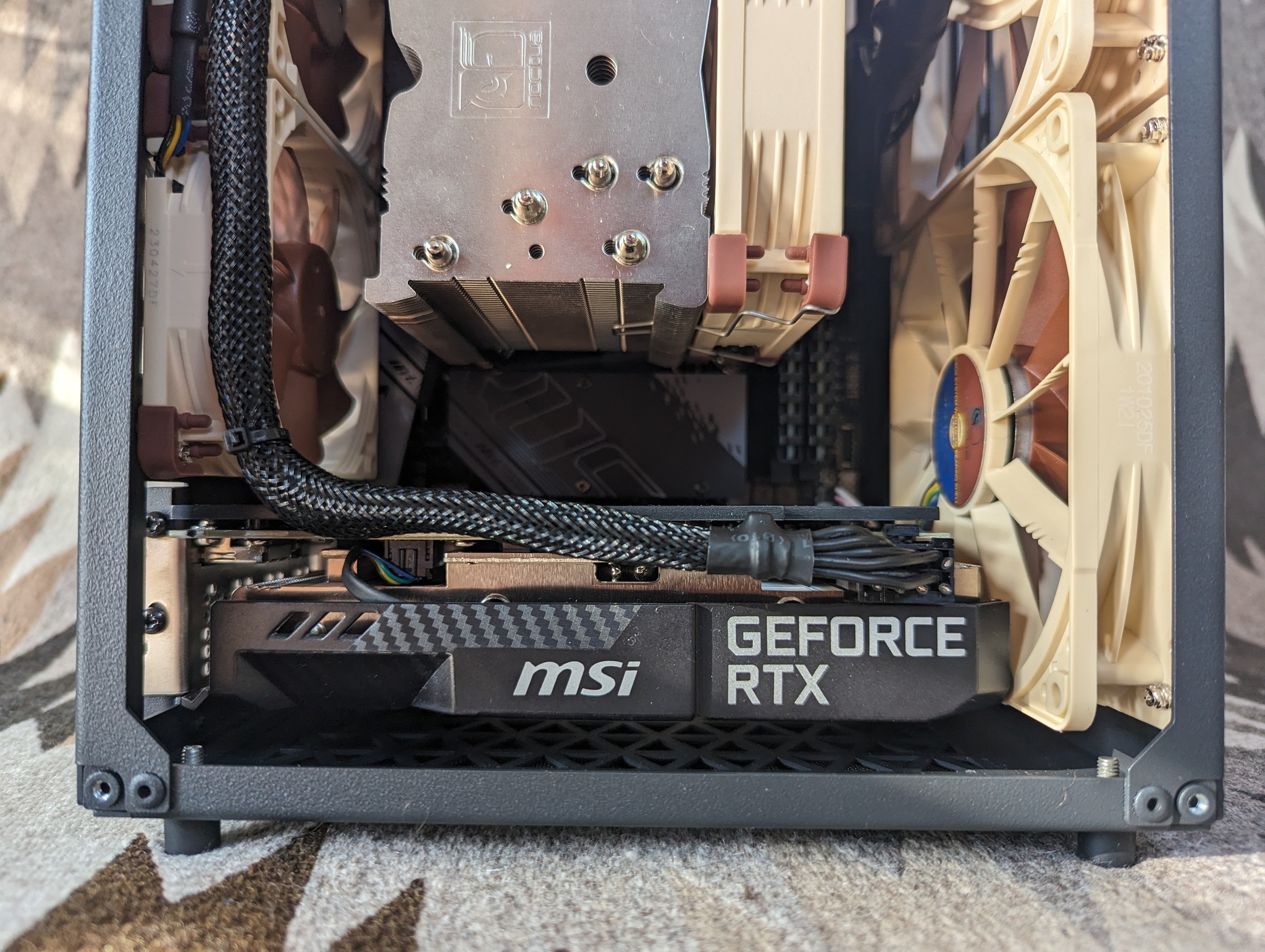
CPU: Intel i9-13900K
Cooler: Noctua NH-U9S
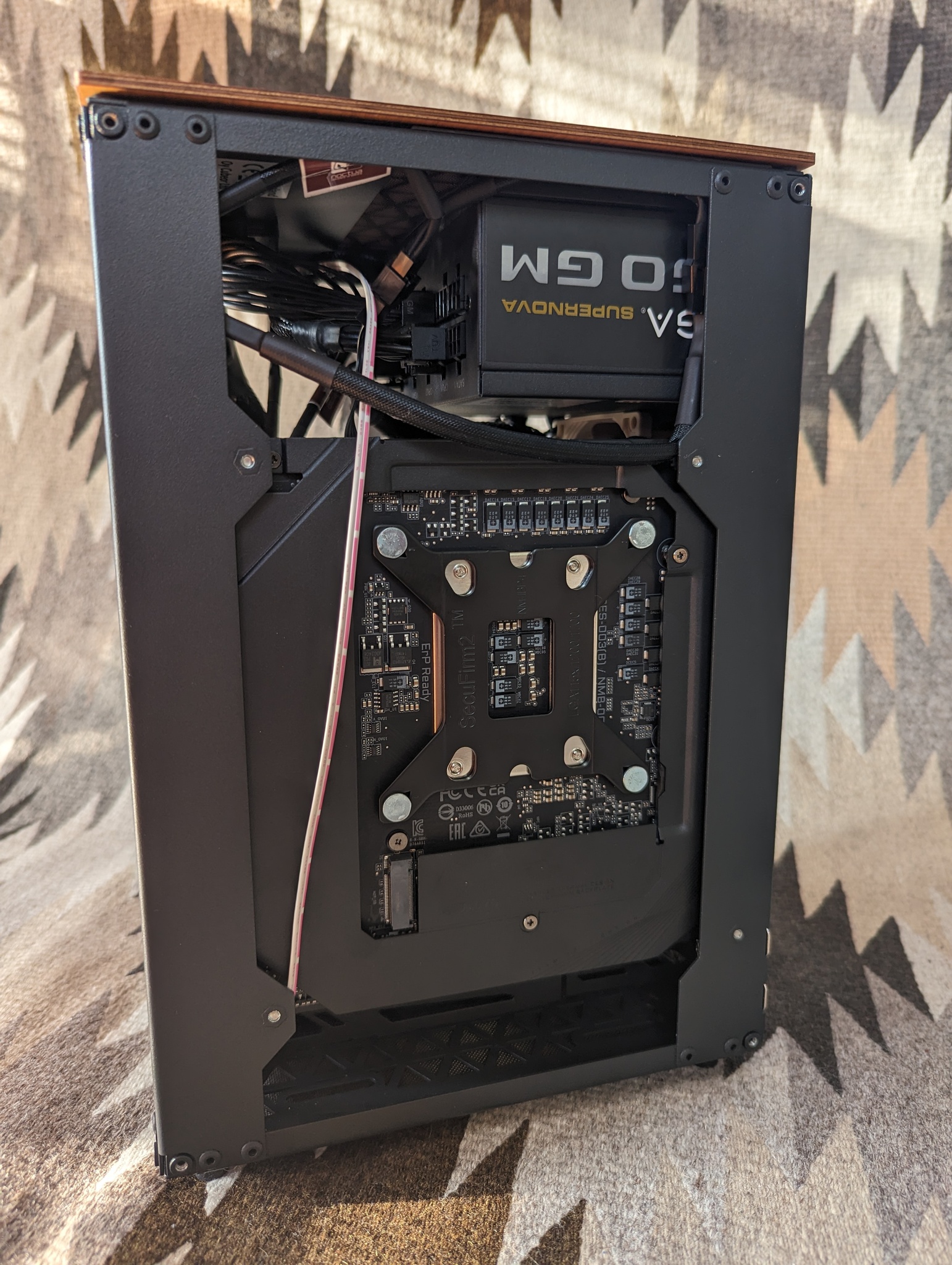
Motherboard: Gigabyte B760I Aorus Pro DDR4
Memory: Corsair Vengeance 64GB DDR4 kit (CL16)
Storage: Samsung 970 EVO 1TB
GPU: MSI RTX 3060 AERO ITX 12G OC
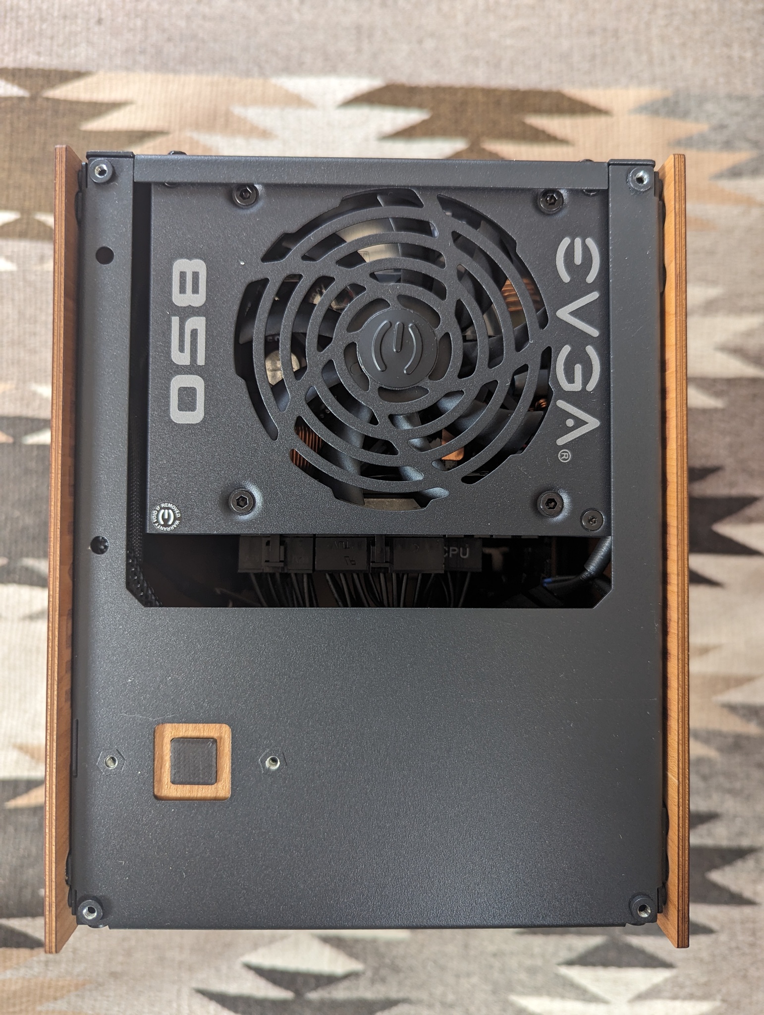
PSU: EVGA SuperNOVA 850 GM
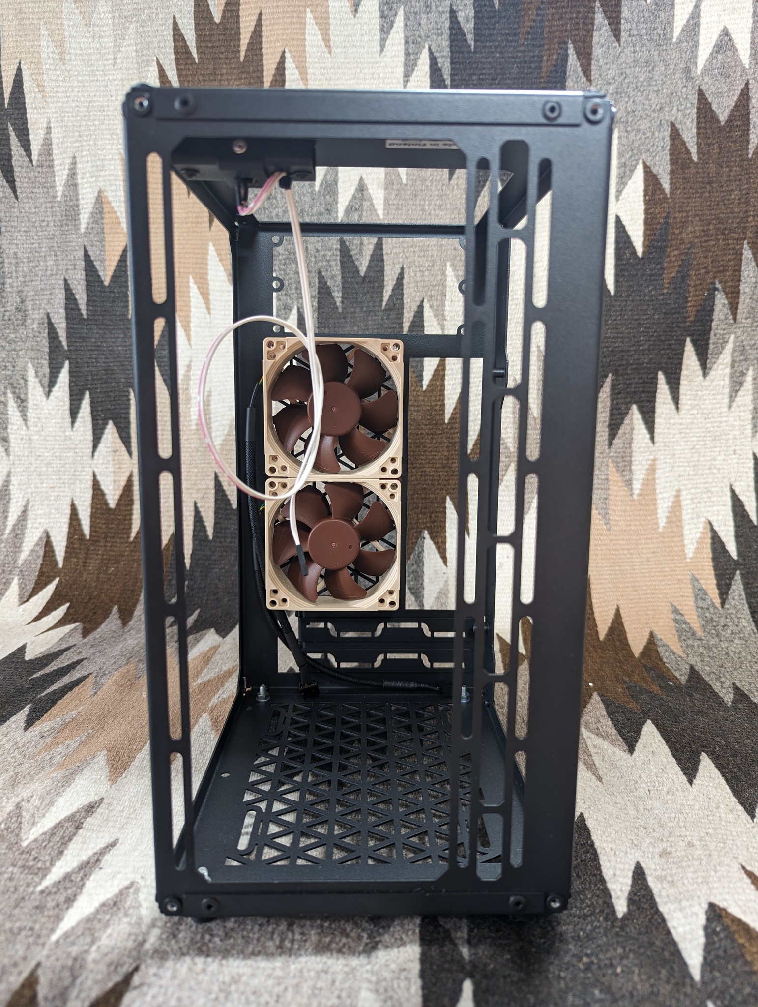
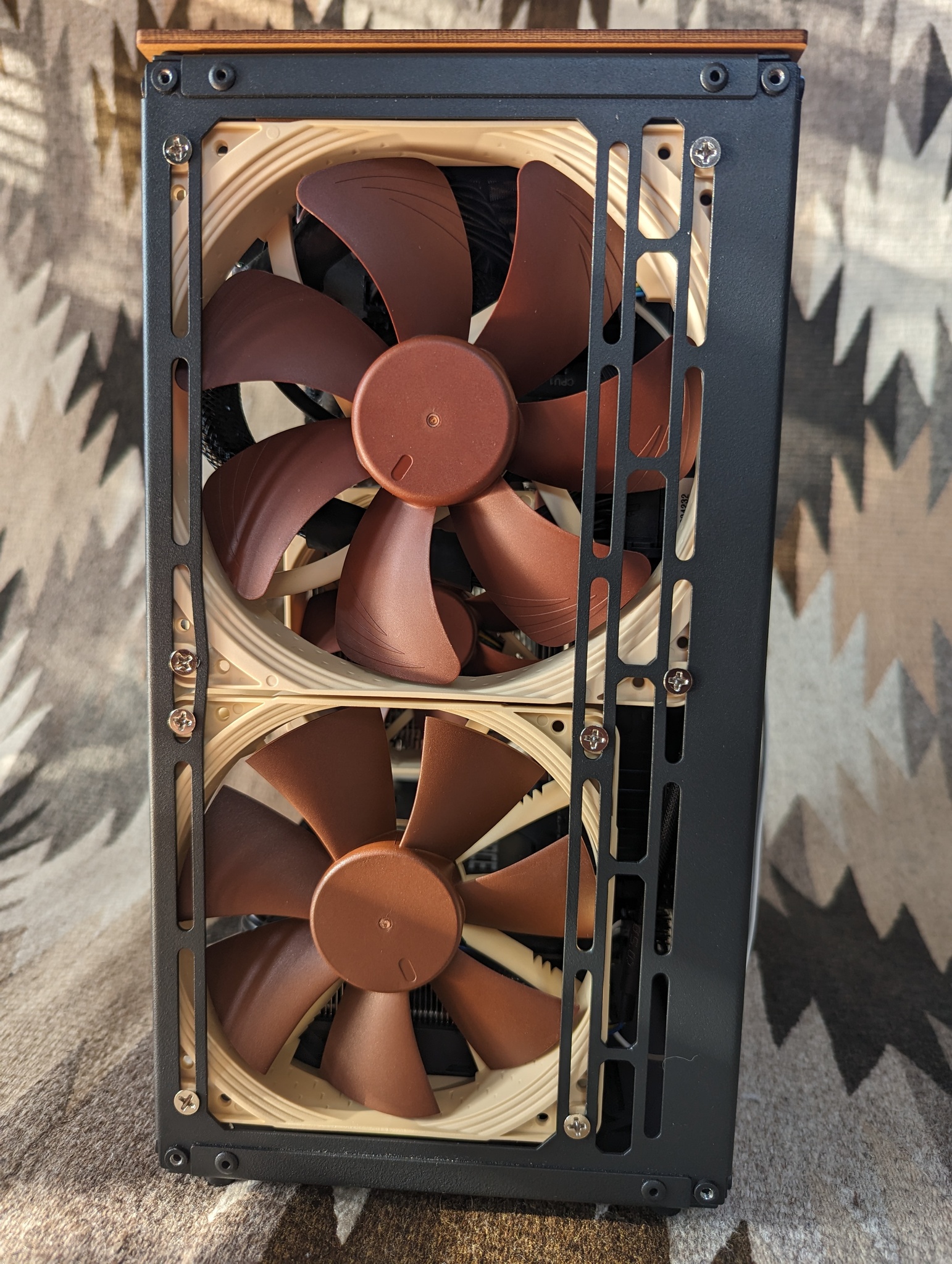
Additional fans:
1x NF-A14 140mm front intake fan (top)
1x NF-F12 120mm front intake fan (bottom)
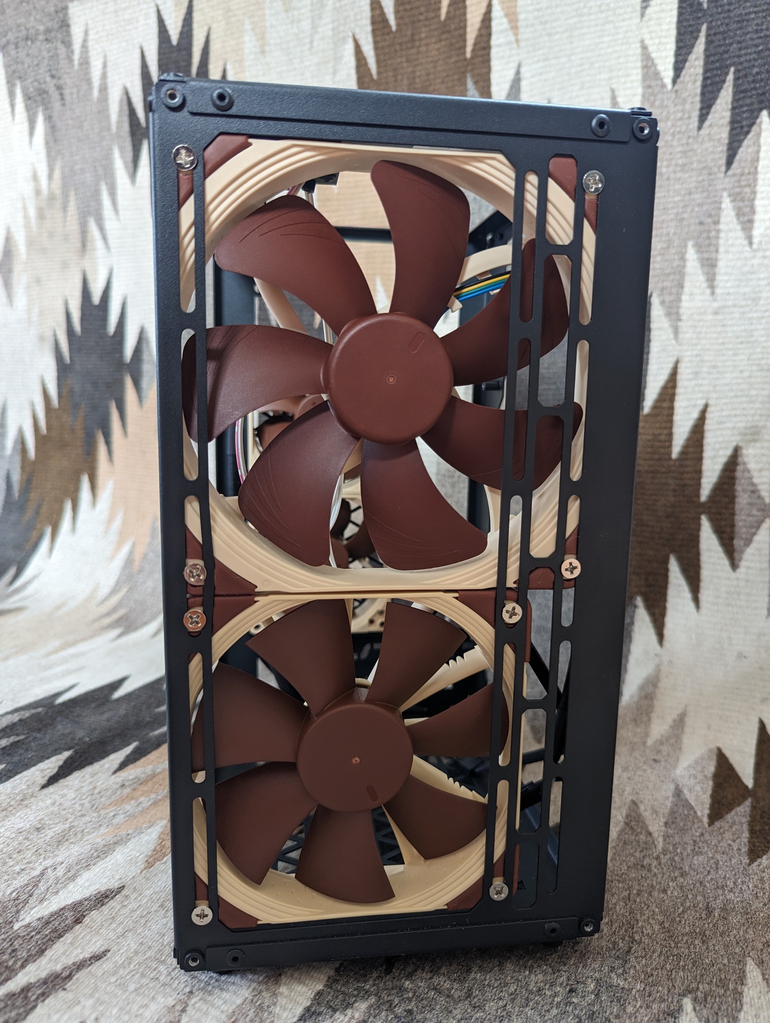
2x NF-A8 80mm rear exhaust fans
The Case
Quick Look
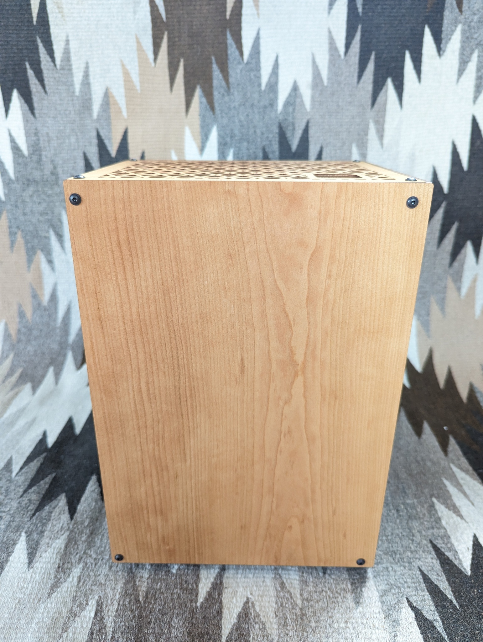
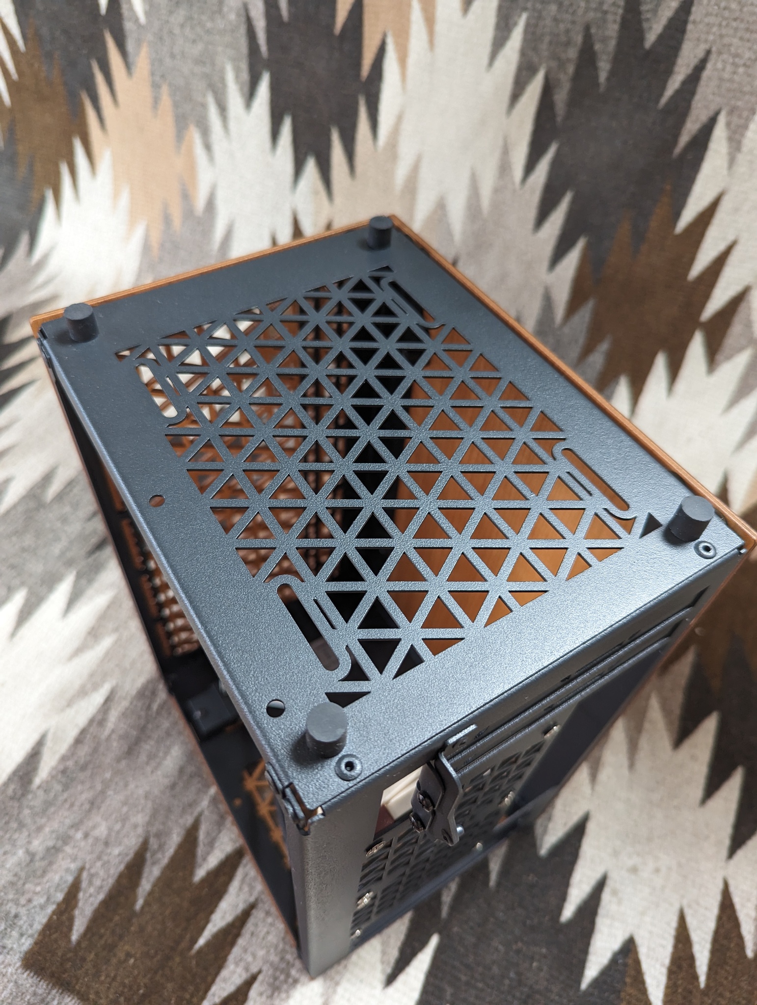
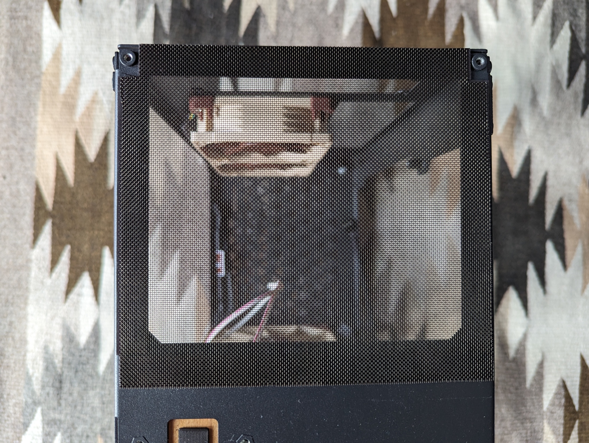
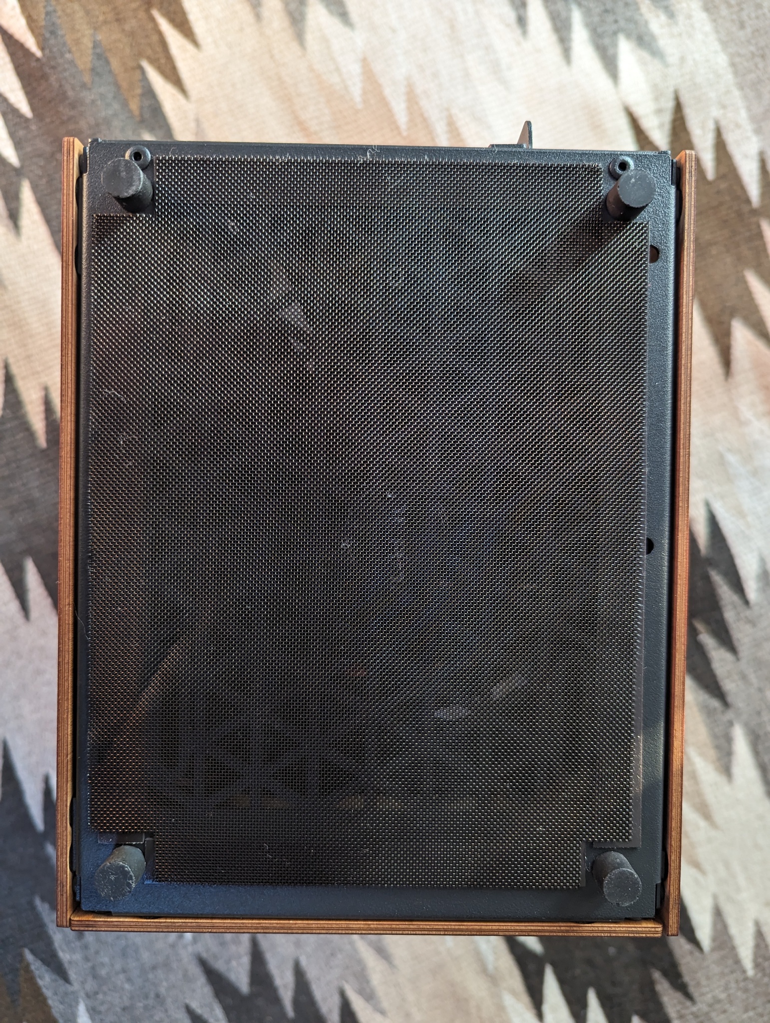
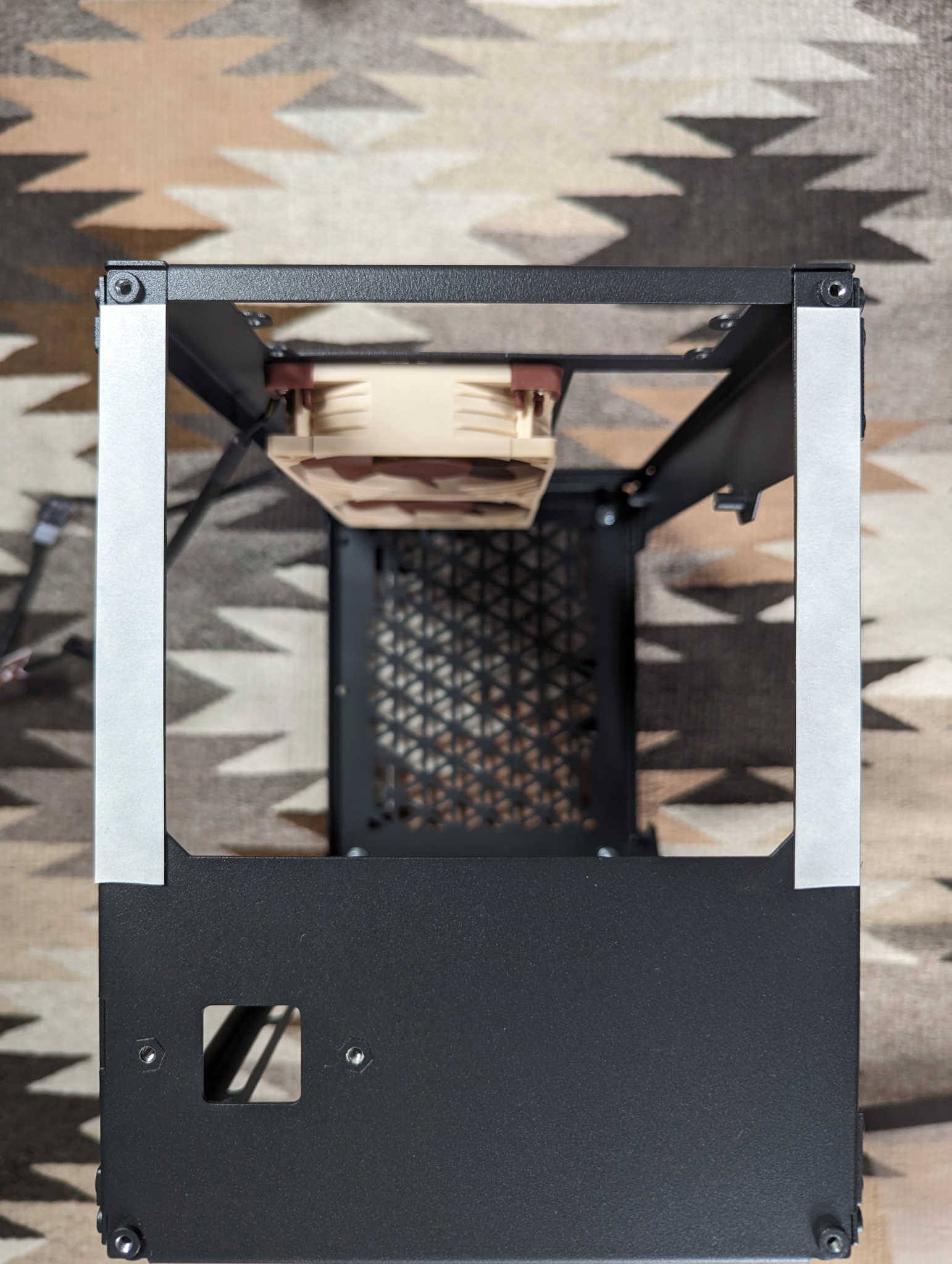
Here are some photos of the case more-or-less as it appears out of the box.
This is the ‘cherry’ colourway for the side panels. Note that the apparent
lightness of the panels will vary as some photos are exposure compensated for
the black elements of the case.
Initial Observations
Shipping cost is pretty reasonable for international, but budget some time for
delivery. I placed my order on July 10th, the case shipped on the 14th, and
arrived on the 24th.
Case arrived fully assembled and nicely packed. There were styrofoam plates
on the top and bottom, and U-shaped spacers on the face and rear to ensure all
sides were stood off from the shipping box. The entire box itself was also
wrapped in some foam packaging material.
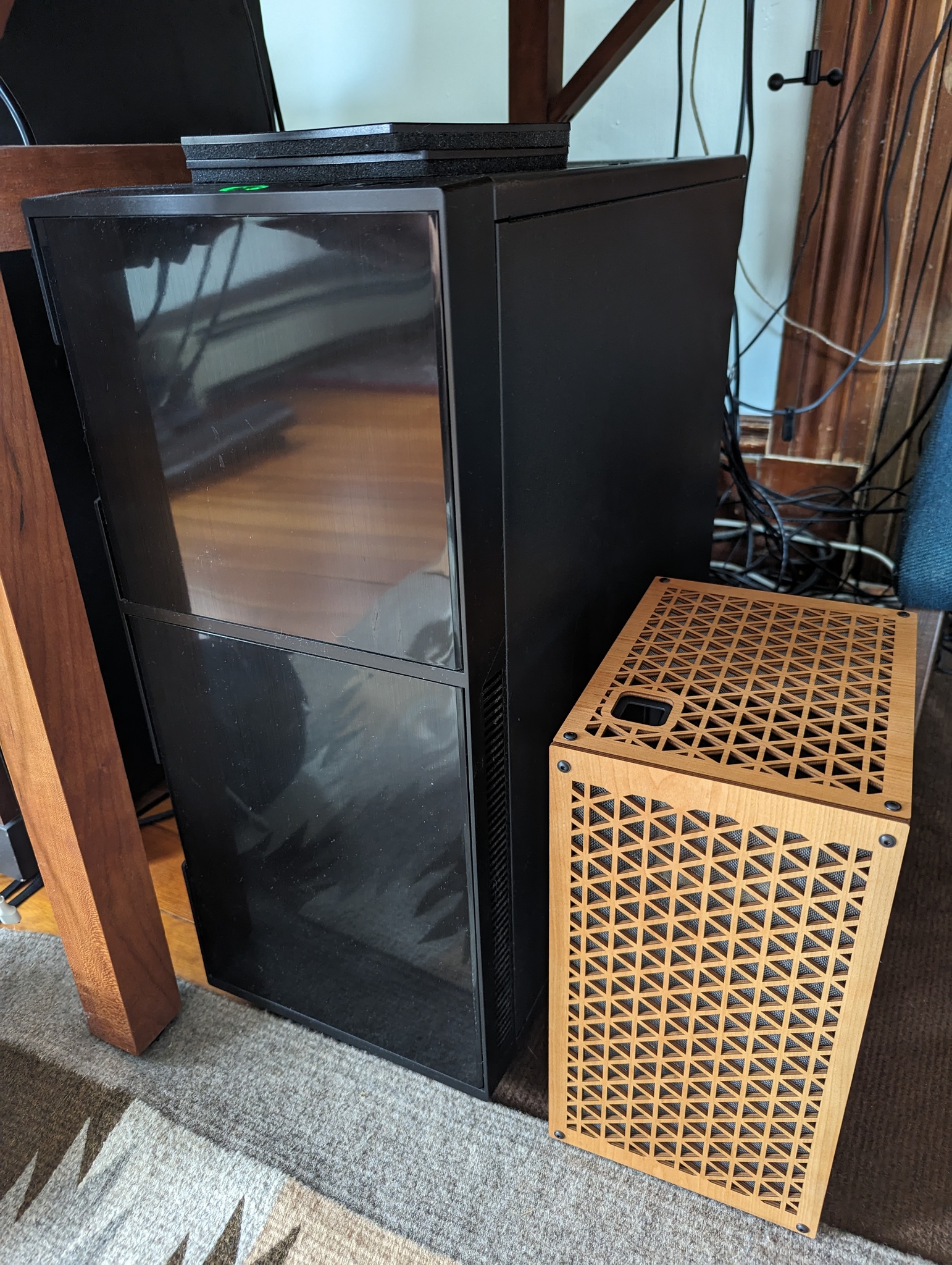
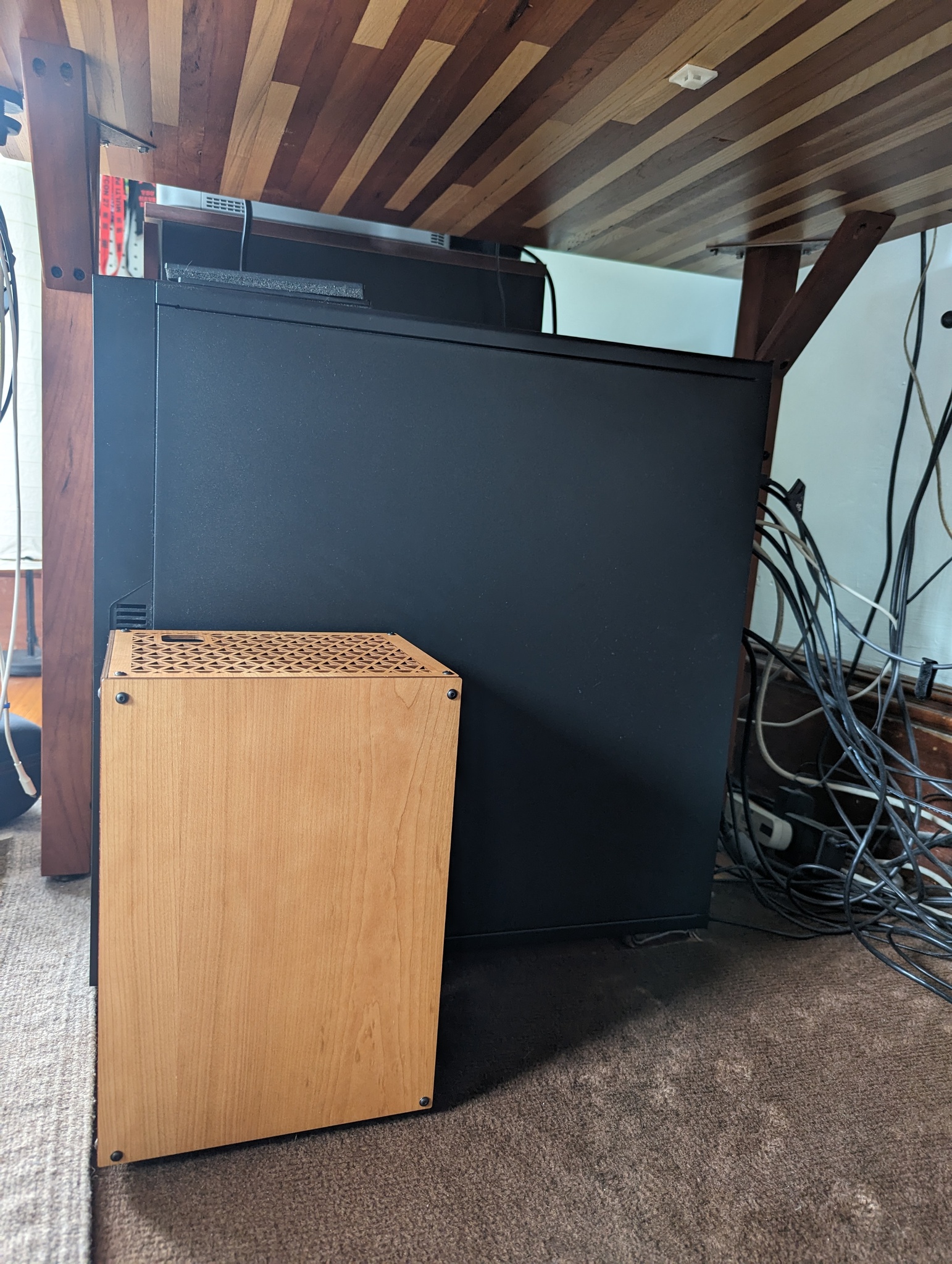
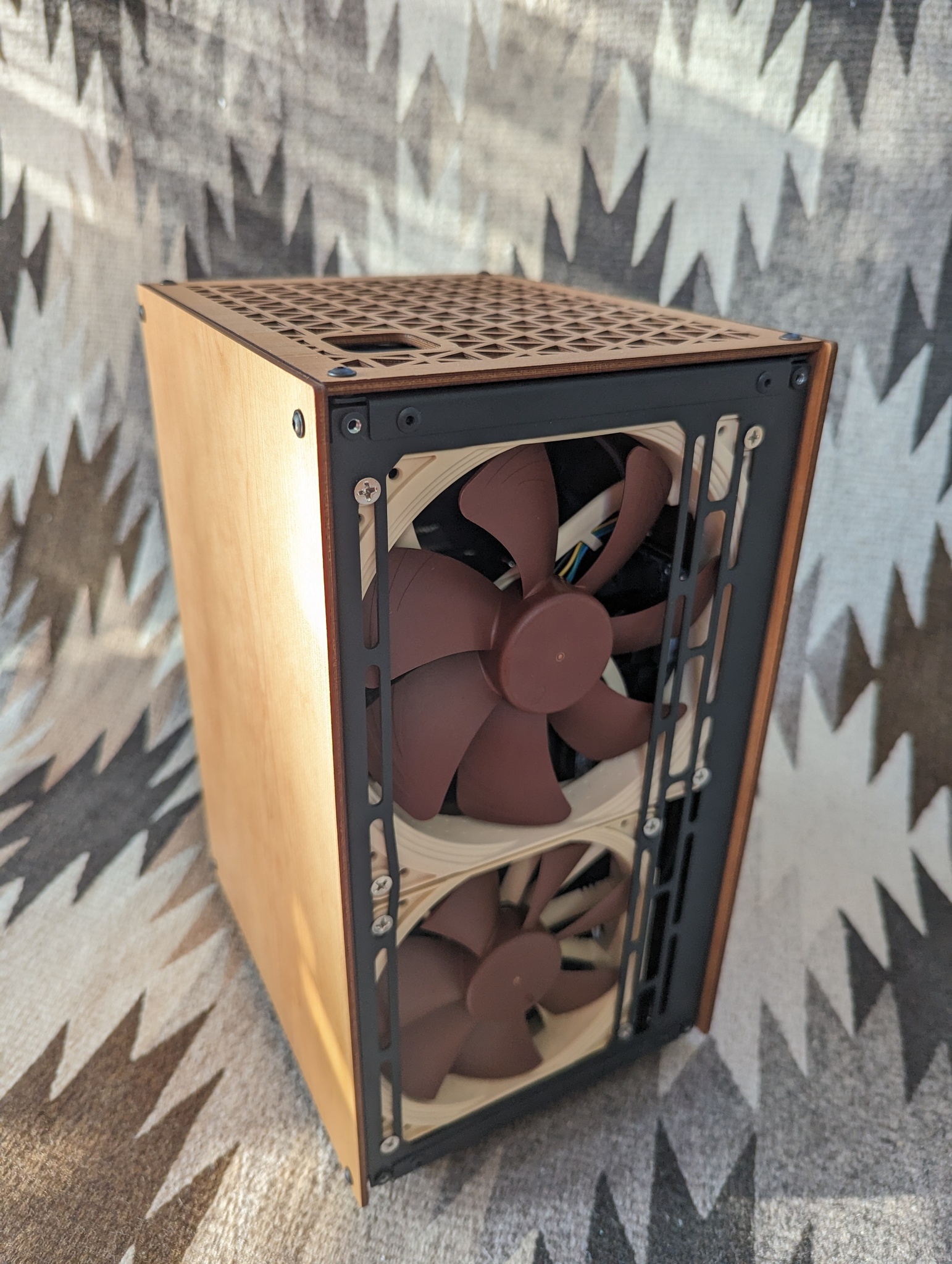
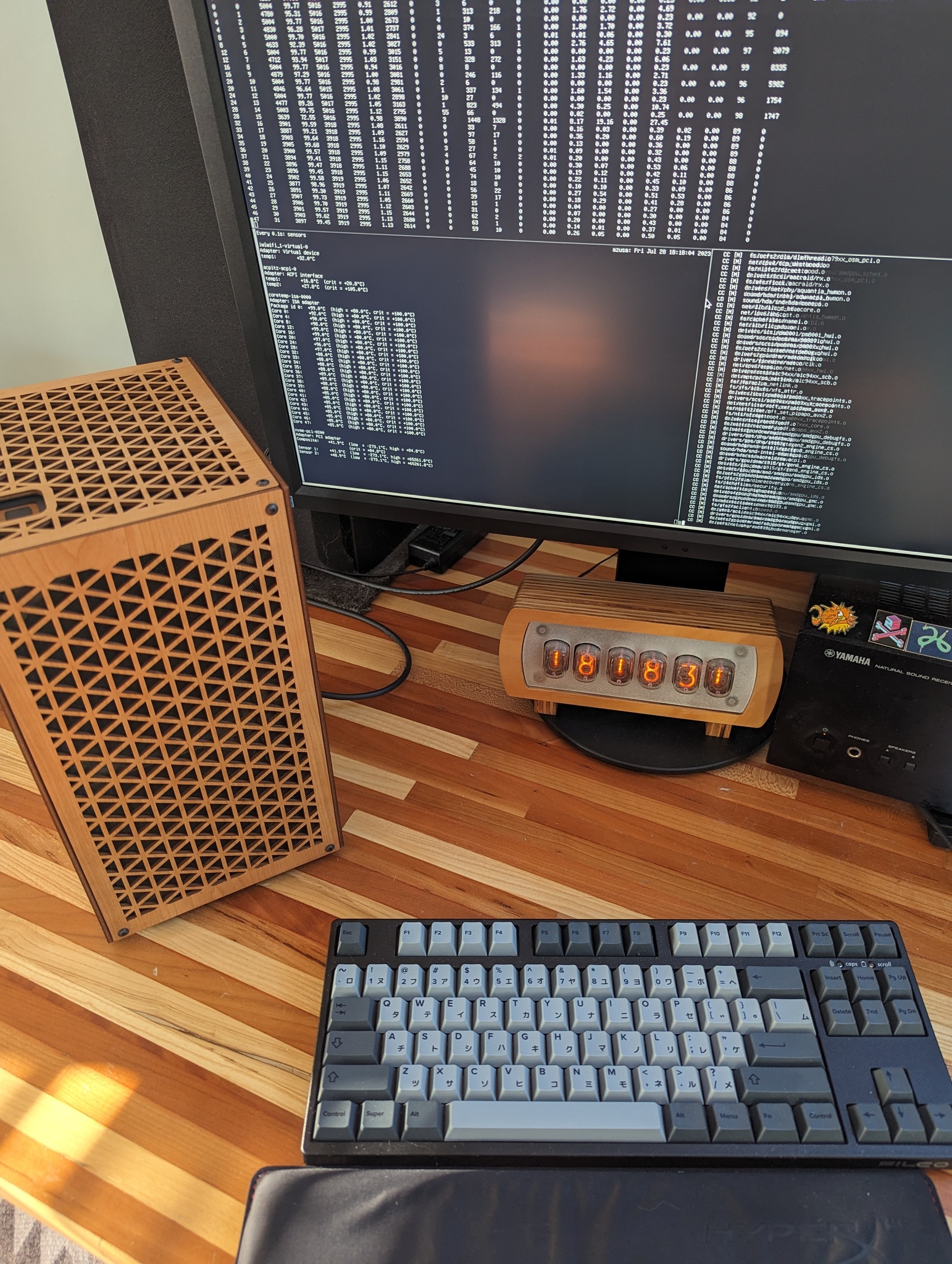
This thing is tiny! Here’s the Aski 2 next to my existing PC, which is
inside a Nanoxia Deep Silence
5,
a case which is about 70L (compared to the Aski 2’s 10L).
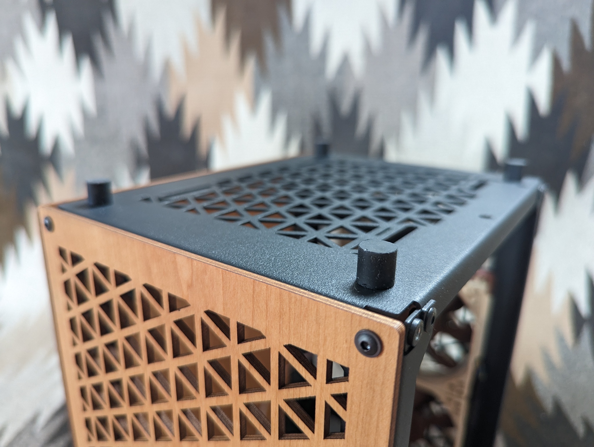
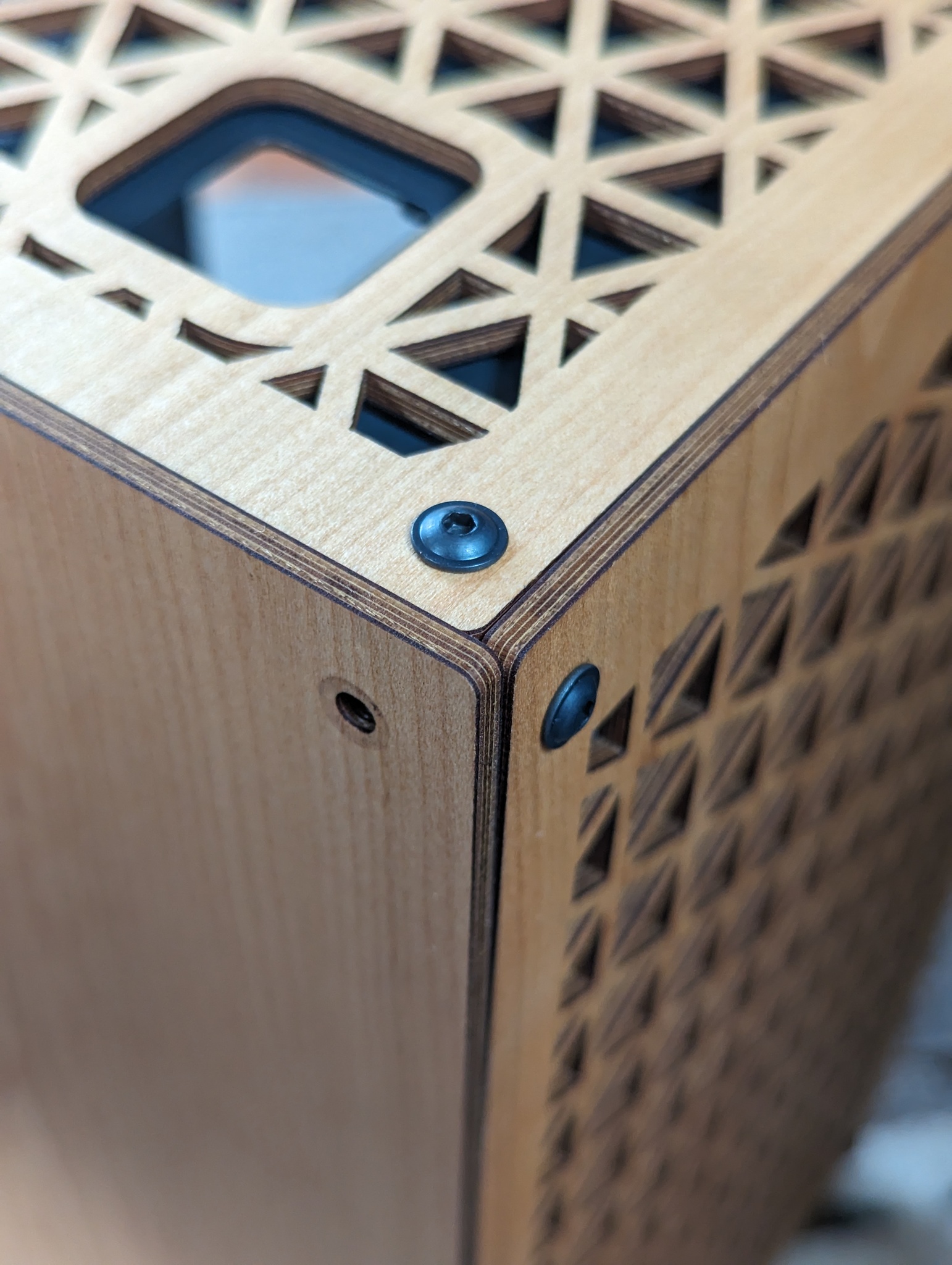
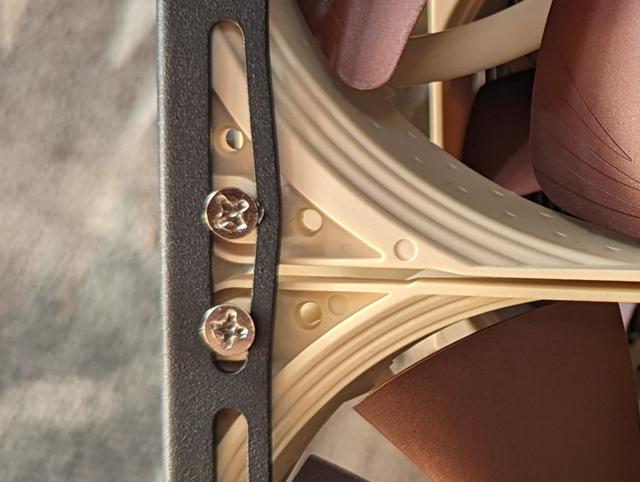
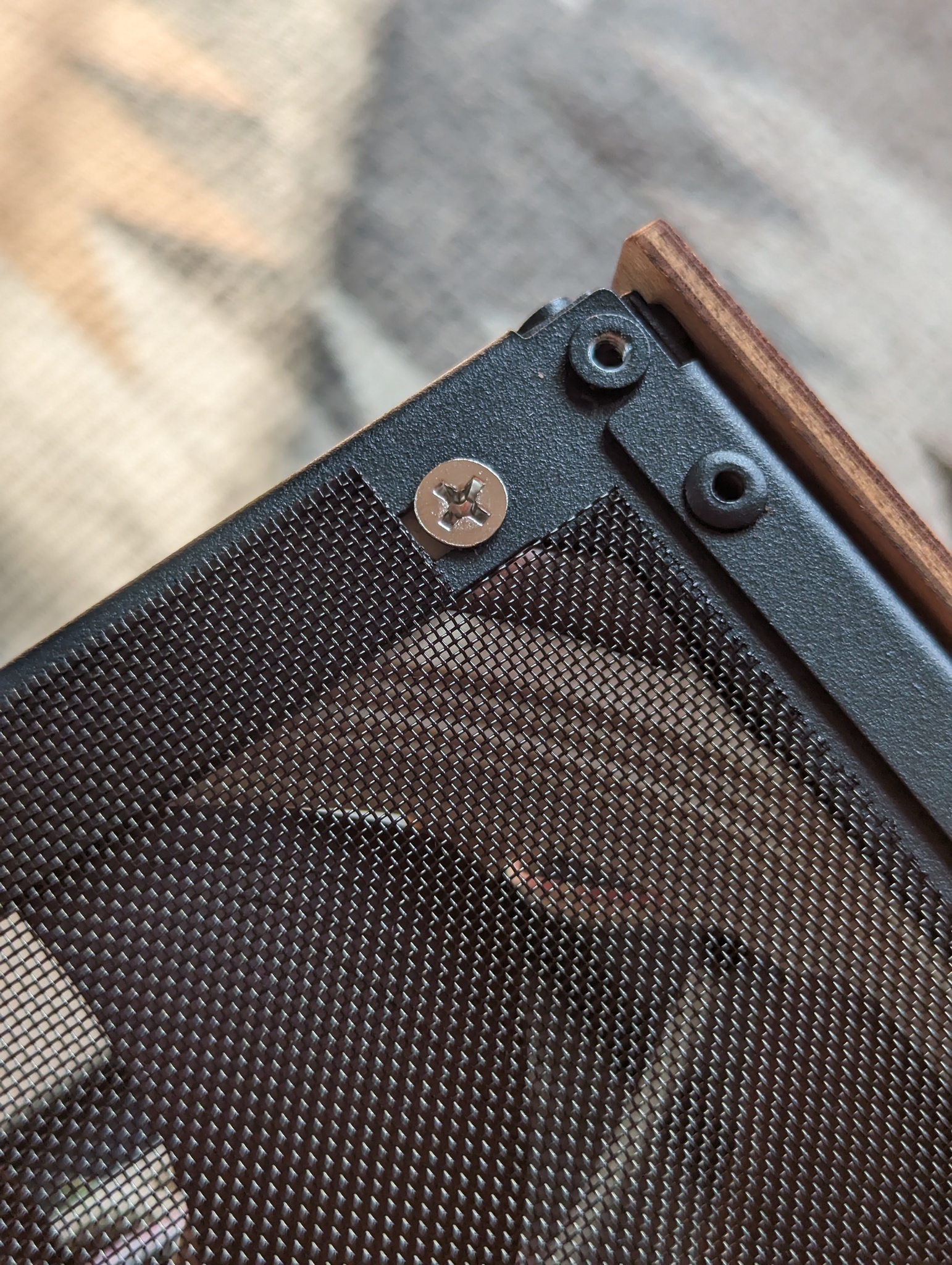
Case panels are affixed with what look M3x6 black flanged button head screws,
so you’ll need a 2mm Allen key. The power button also uses M3 screws, but
slightly longer ones (M3x10). The power button can be easily removed if
necessary to wrangle the PSU.
The case doesn’t come with any motherboard mounting screws, and my
motherboard only came with whatever thread screws come with ordinary ATX cases.
The standoffs on the Aski 2 are M3 thread, though the thread starts
surprisingly far down the standoff - there’s about 4mm of unthreaded lead-in.
Not sure what purpose this serves, but I had some M3x12 button heads lying
around, so I used 4 of these to secure the motherboard.
The top of the standoffs are about 9mm from the top face of the internal metal
panel, which leaves a little bit of room on the back for hiding cables.
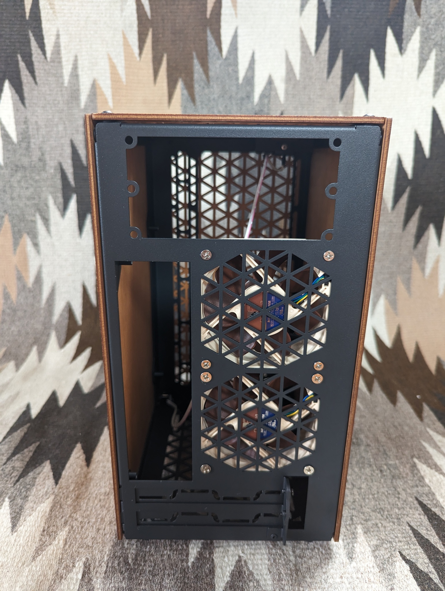
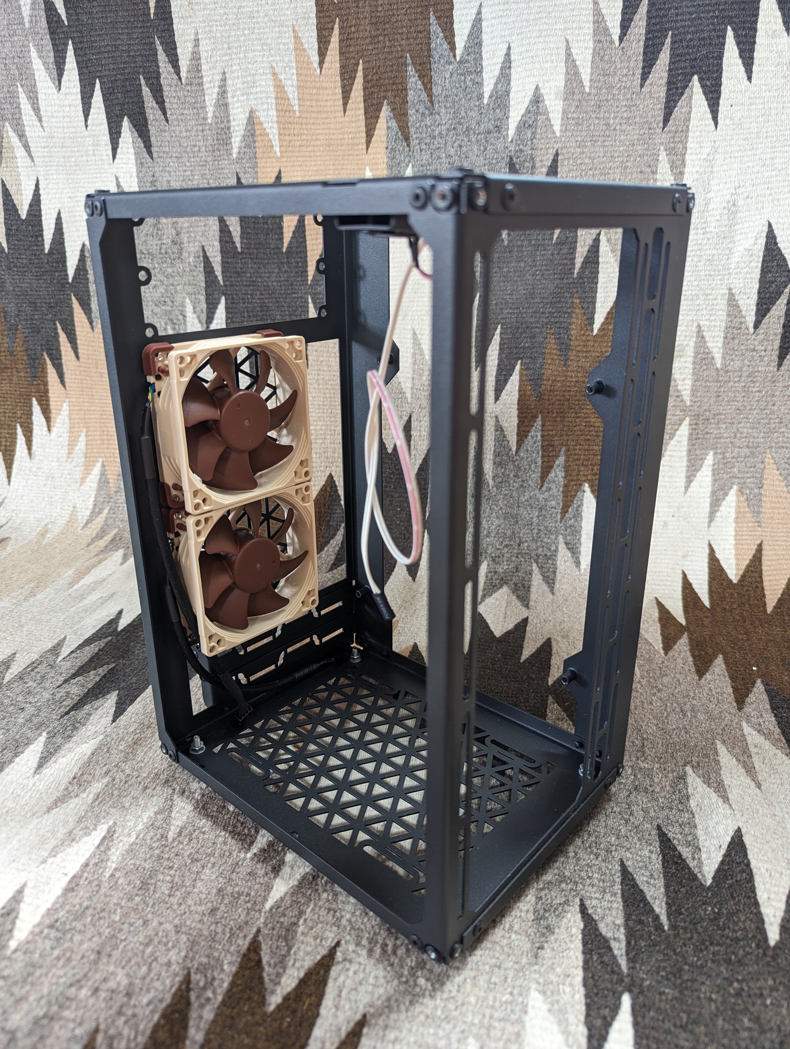
The internal metal structure feels very sturdy. No flex at all. Riveted
construction.
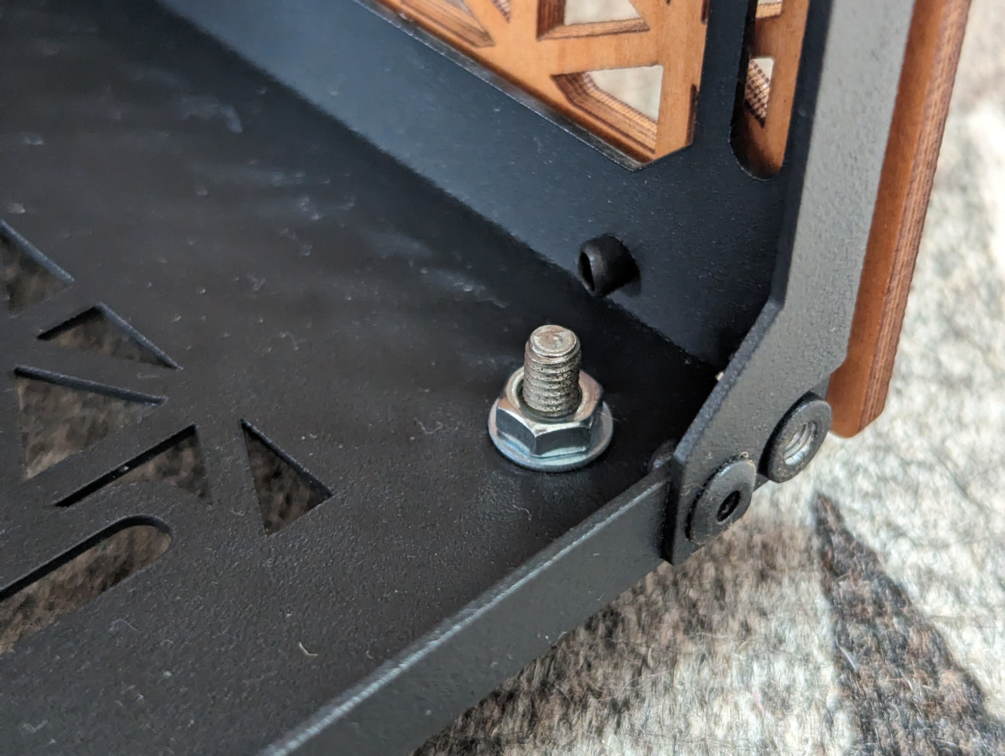
I got the extended feet, which are 10mm of rubber with a 10mm M4 threaded
screw. They’re attached with a washer and ordinary nut; I’m personally a lock
nut person but I doubt these are going anywhere. The screw is a bit longer than
necessary (10mm is just a standard size), but it’s not like they’re going to
interfere with a GPU mount.
You could get different feet off McMaster if you really wanted to (e.g. something like
this, so you just have the head of your
screw in the case instead of the thread), but the durometer on the provided ones
feels pretty good for a PC foot.
Foot thread extends into case slightly more than needed
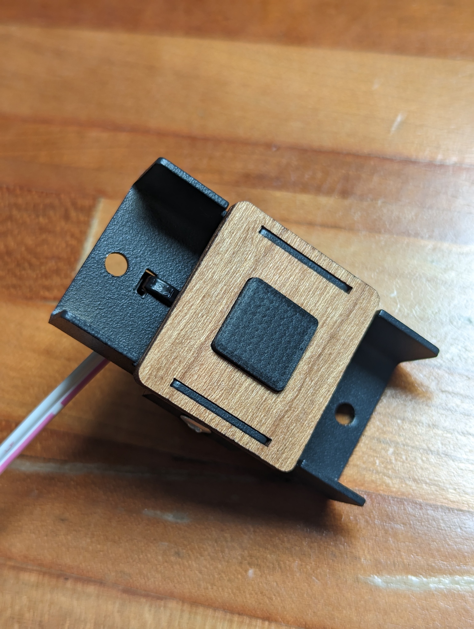
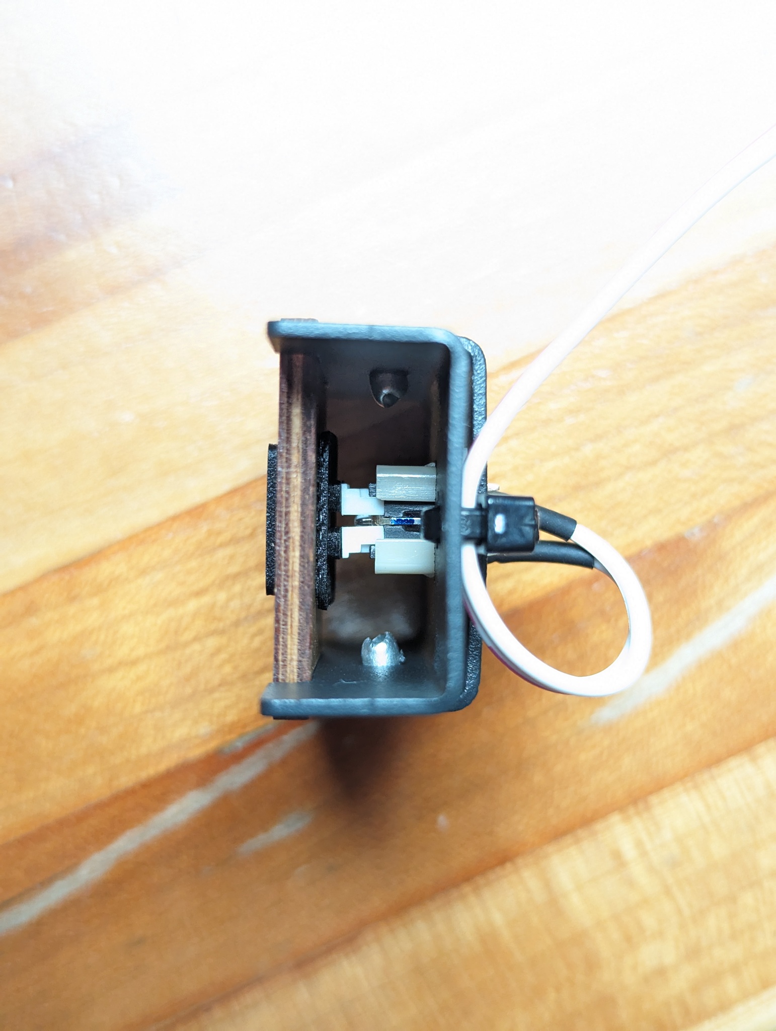
The power button assembly is very cute. Comes off easily with two M3x10
screws. The physical actuator is 3d printed, but has a reasonably nice finish.
We’ll see how it holds up; the fact that I can see the internal structure does
make me worry it might delaminate or something with heavy use. That said, this
is a button that’s getting pressed on the order of once a day. The switch
itself is a tactile momentary switch that clips into the larger U-channel metal
piece and then seems to be sandwiched by the smaller. Unfortunately this second
piece is riveted in place, so replacing the tactile switch itself would be a
little inconvenient, but again, very low duty part.
The wood finish plate seems to be a press fit over the larger U-channel. Feels
nice and snug now, though it’s a humid Boston summer, so possible that in a dry
winter it may have more play with the lower humidity.
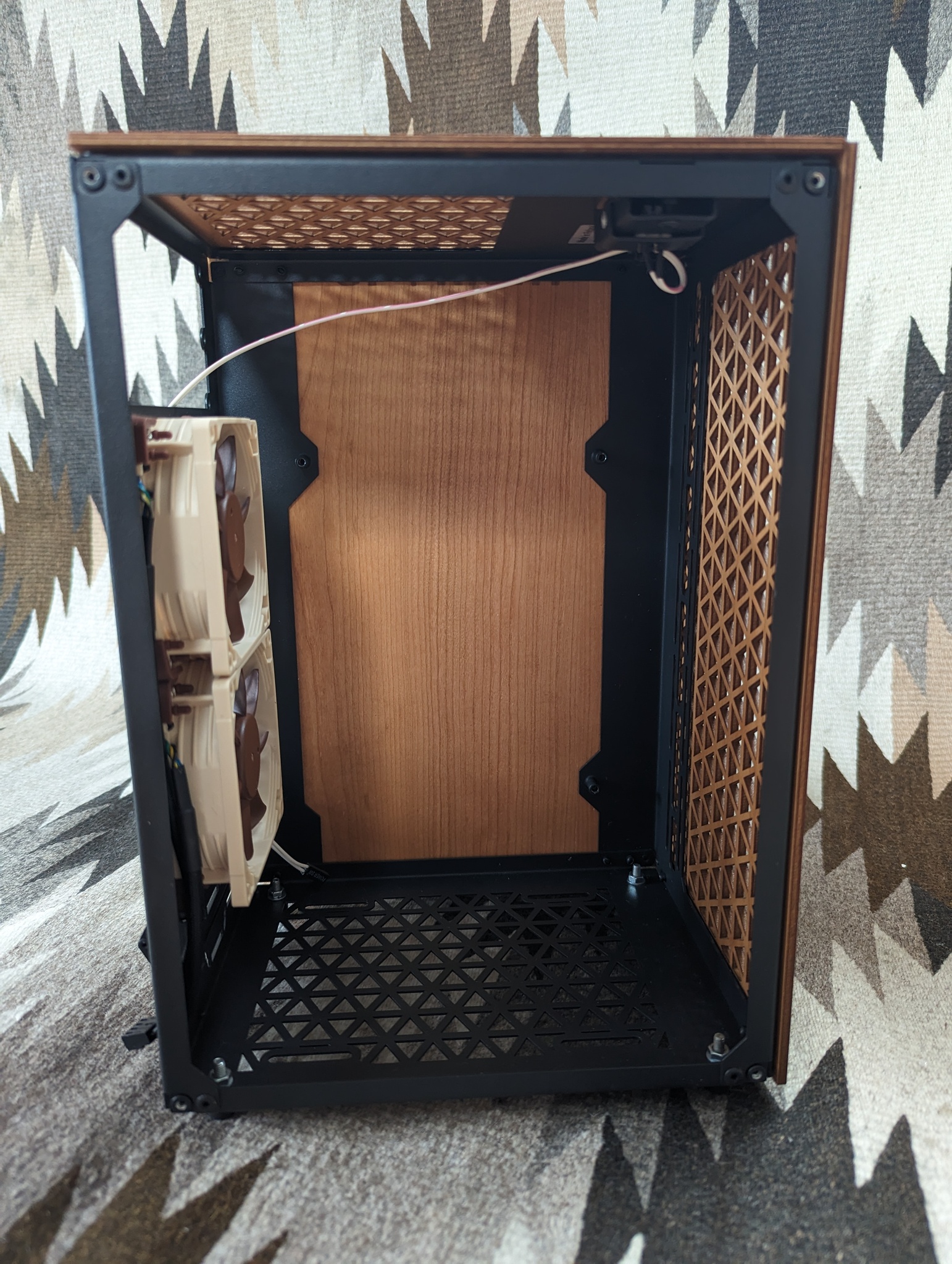
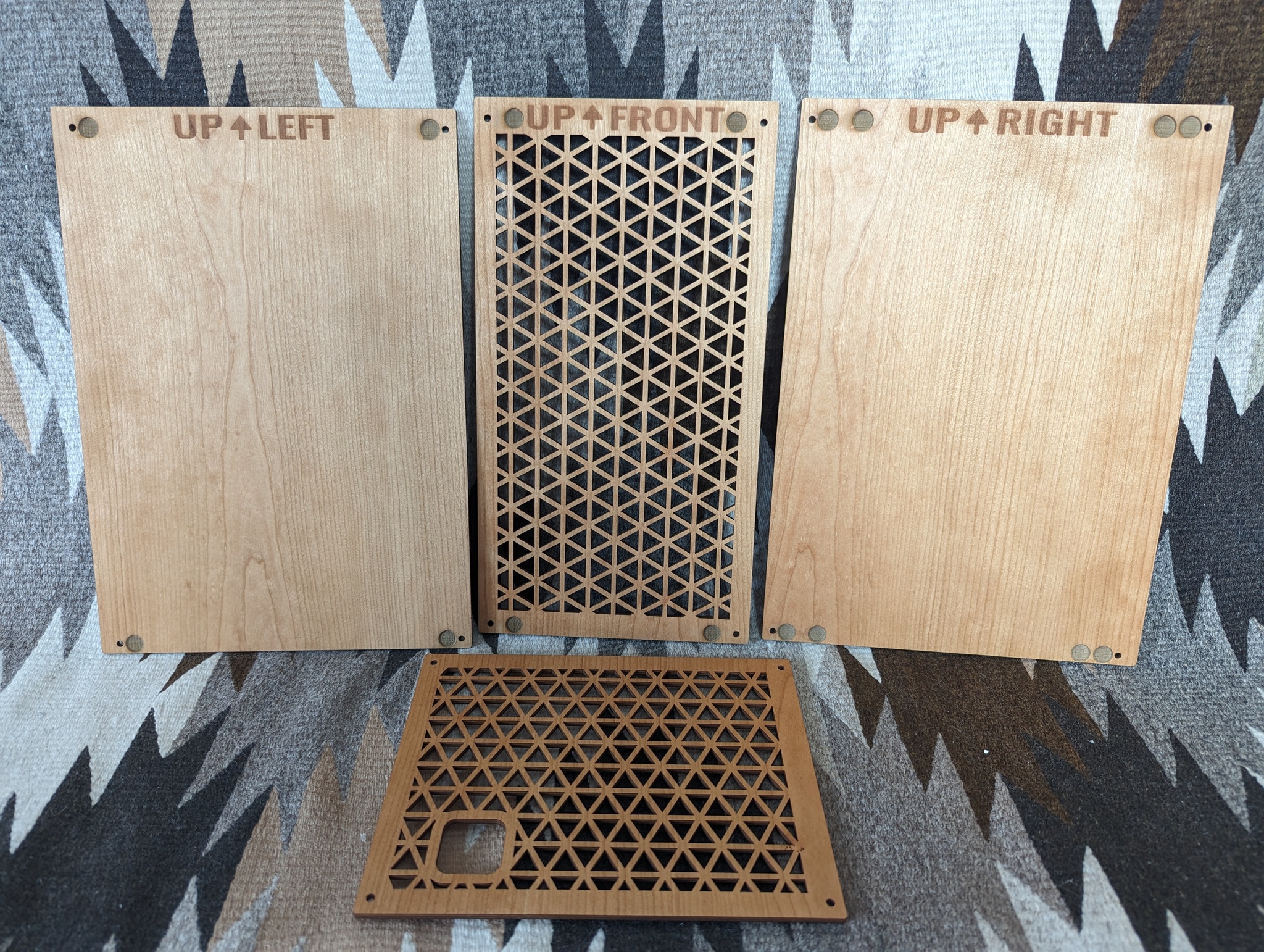
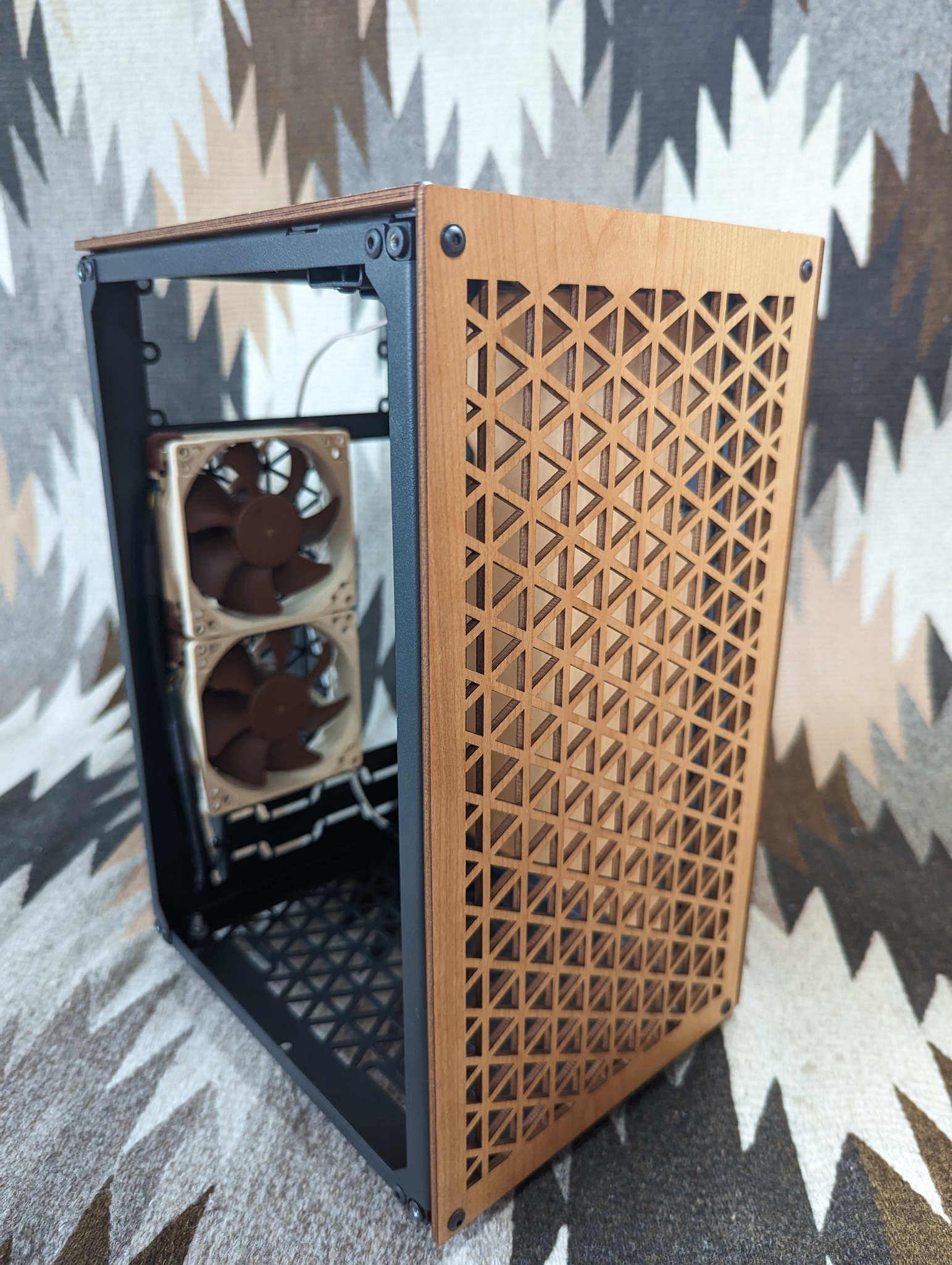
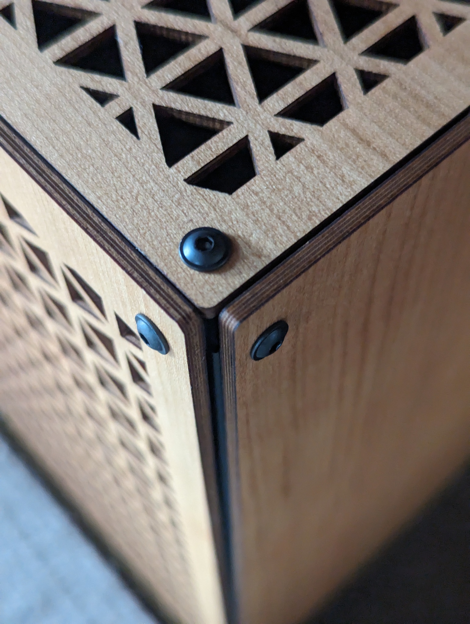
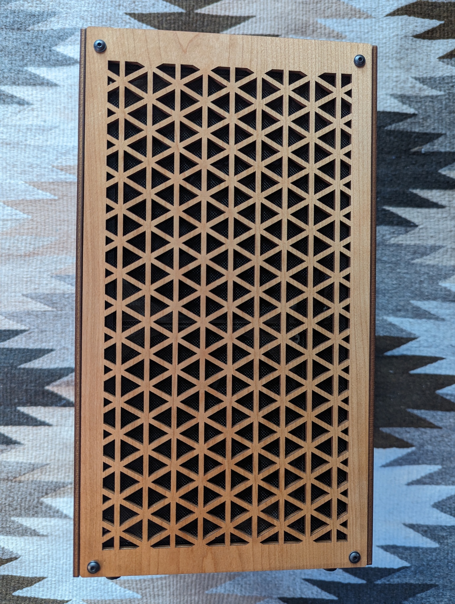
Taking the wood panels off, you can see that they’ve all been cleanly
labelled with which panel it is and which way is up. This is actually
important, because the side panels aren’t identical - they will not line up
perfectly if installed backwards (see photos). When correctly installed, the
panels have very nice tight clearances to each other.
The panels also have little half-lasered holes to avoid interference with the rivets, which is a lovely
touch. You’ll also see in the first photo below that the screws do leave little
marks on the wood, but this is obviously covered by the screw head when
installed.
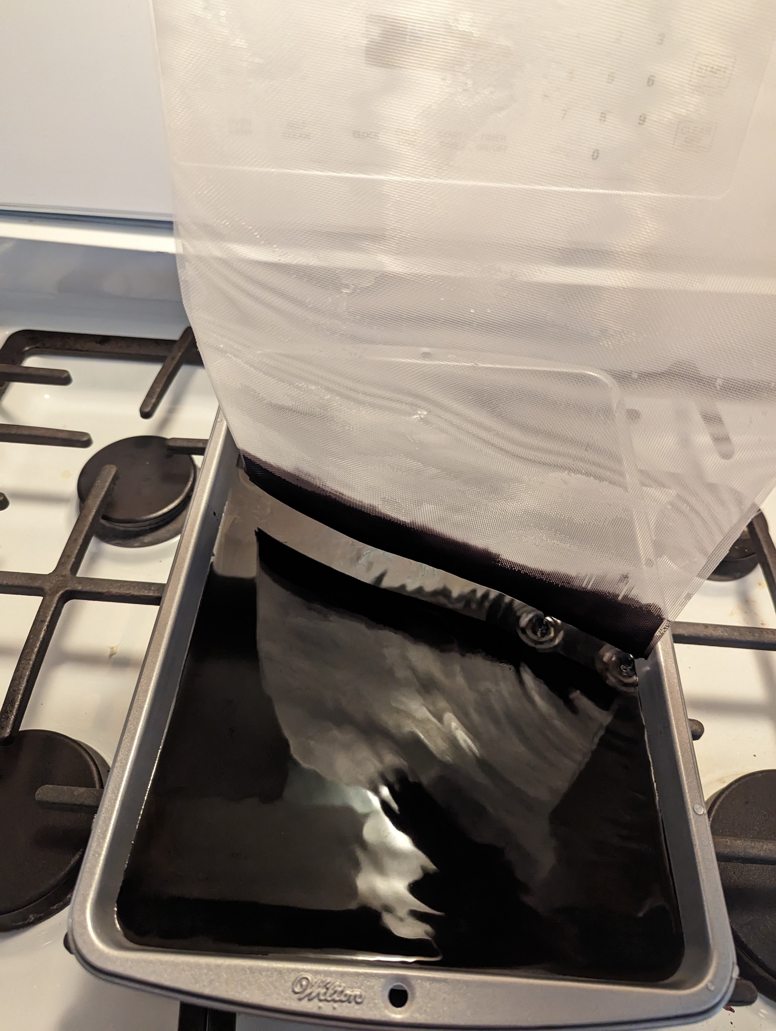
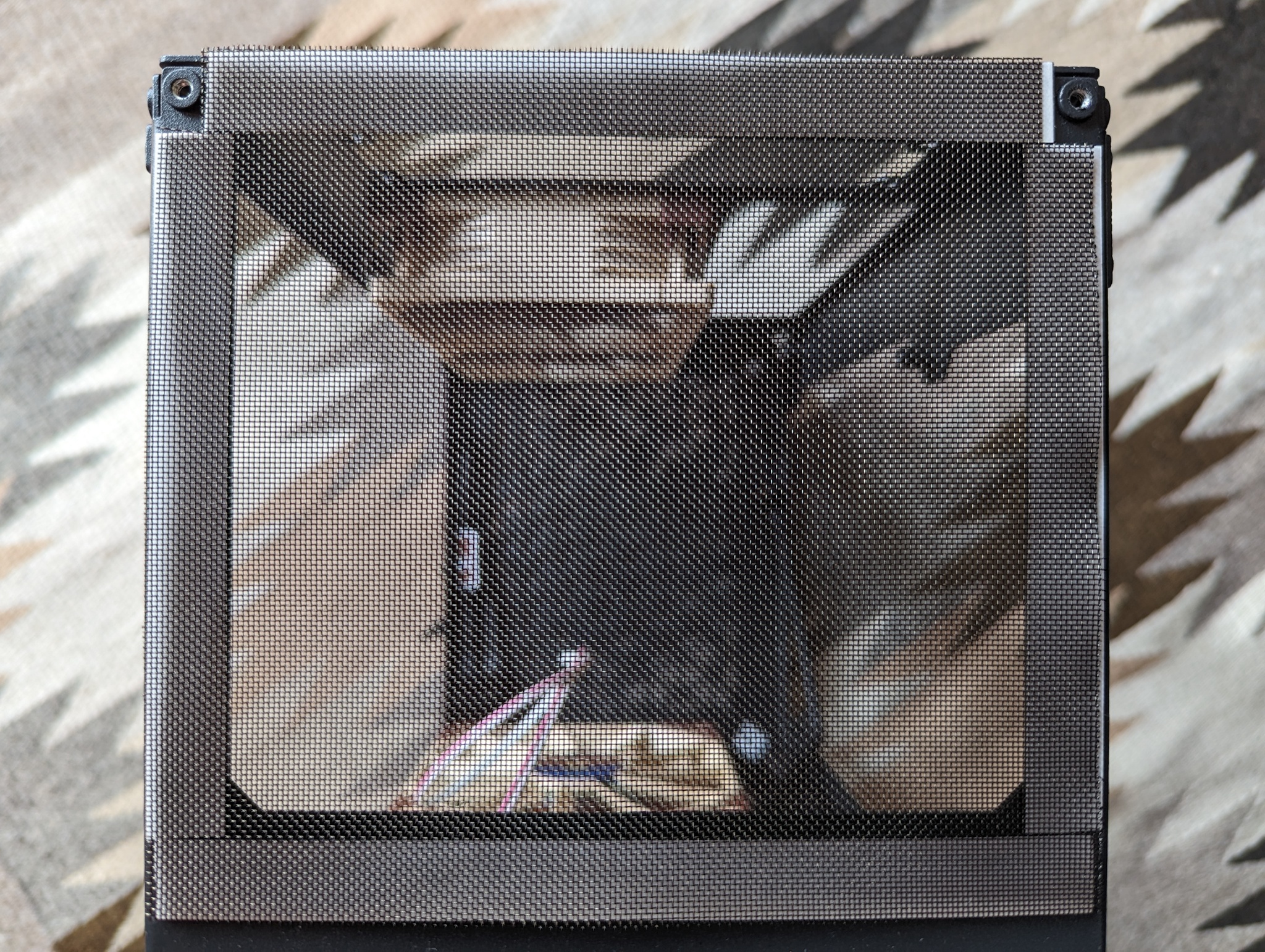
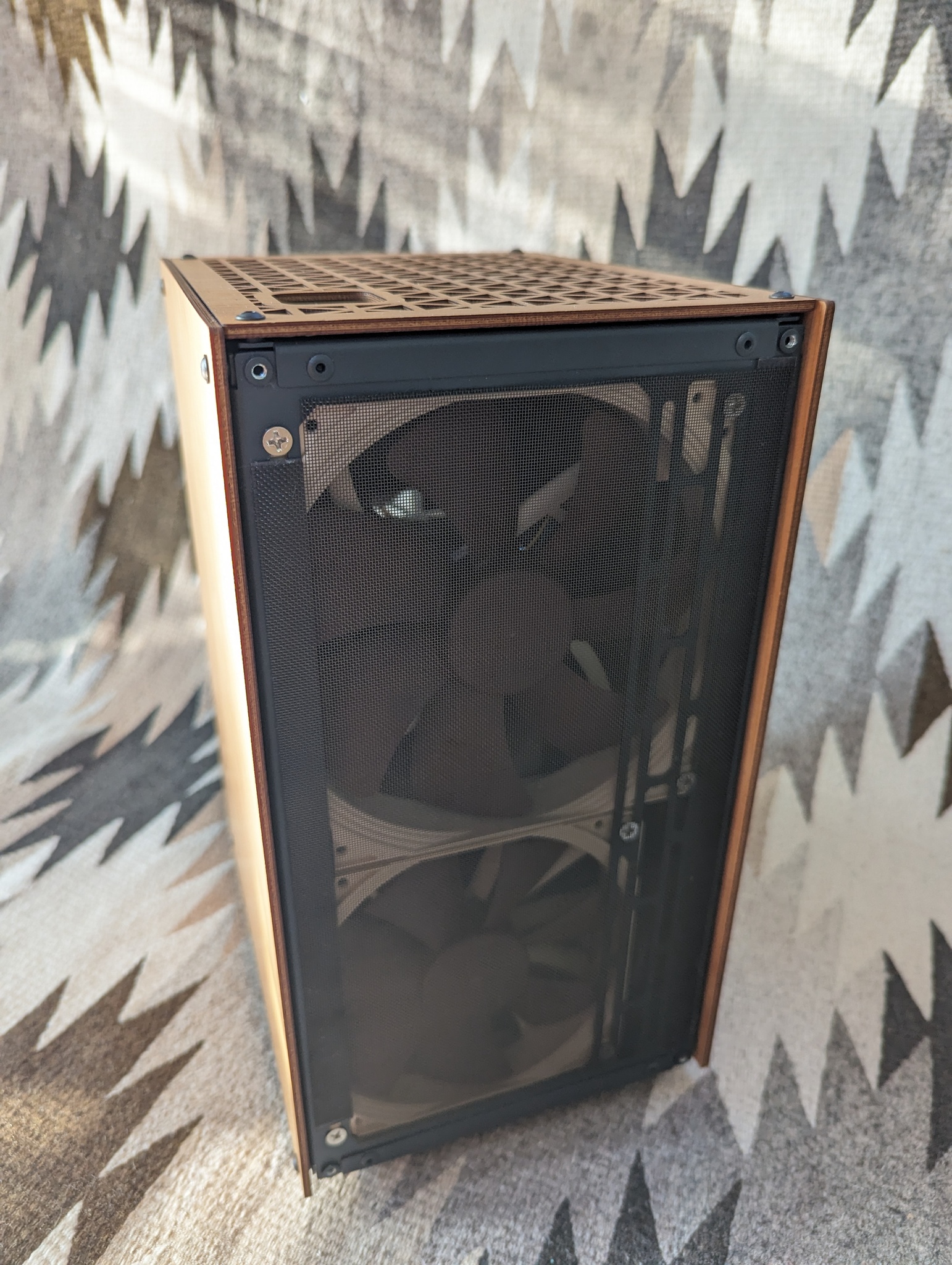
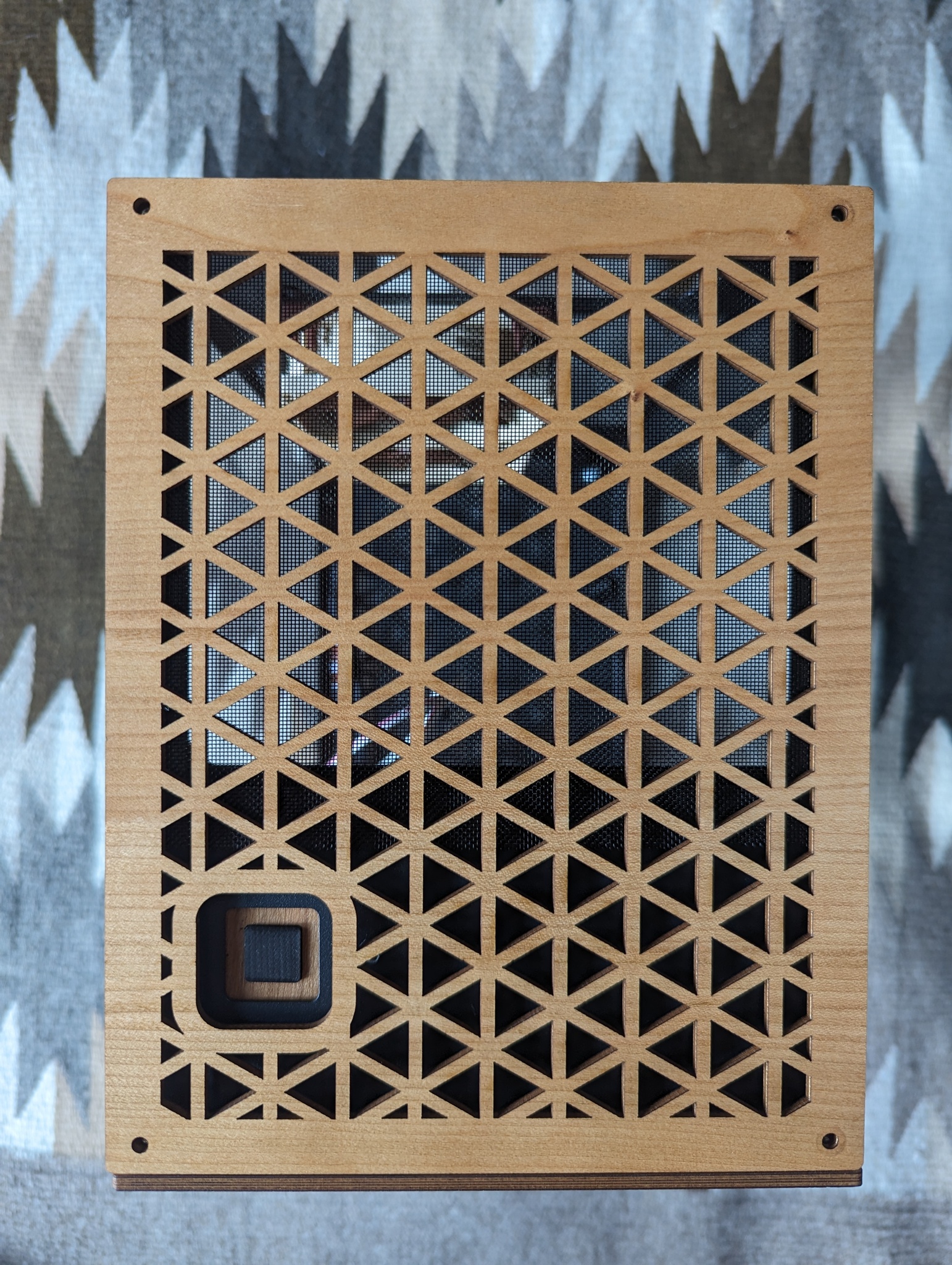
One downside to this case is that it doesn’t come with any fan filters -
luckily it ended up being fairly straightforward to add some in after the fact,
but some sort of integrated solution might be nice for those that live with
pets.
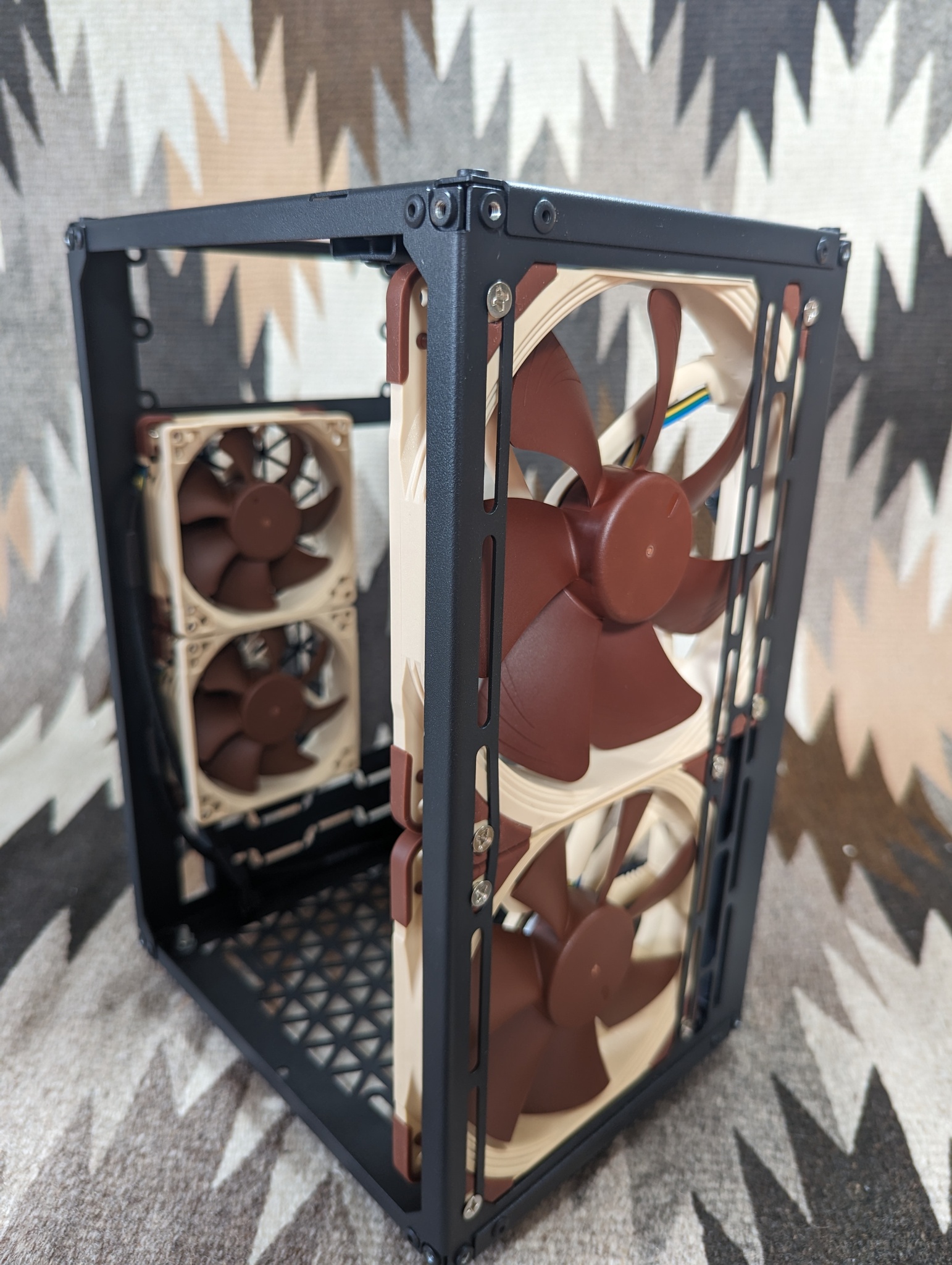
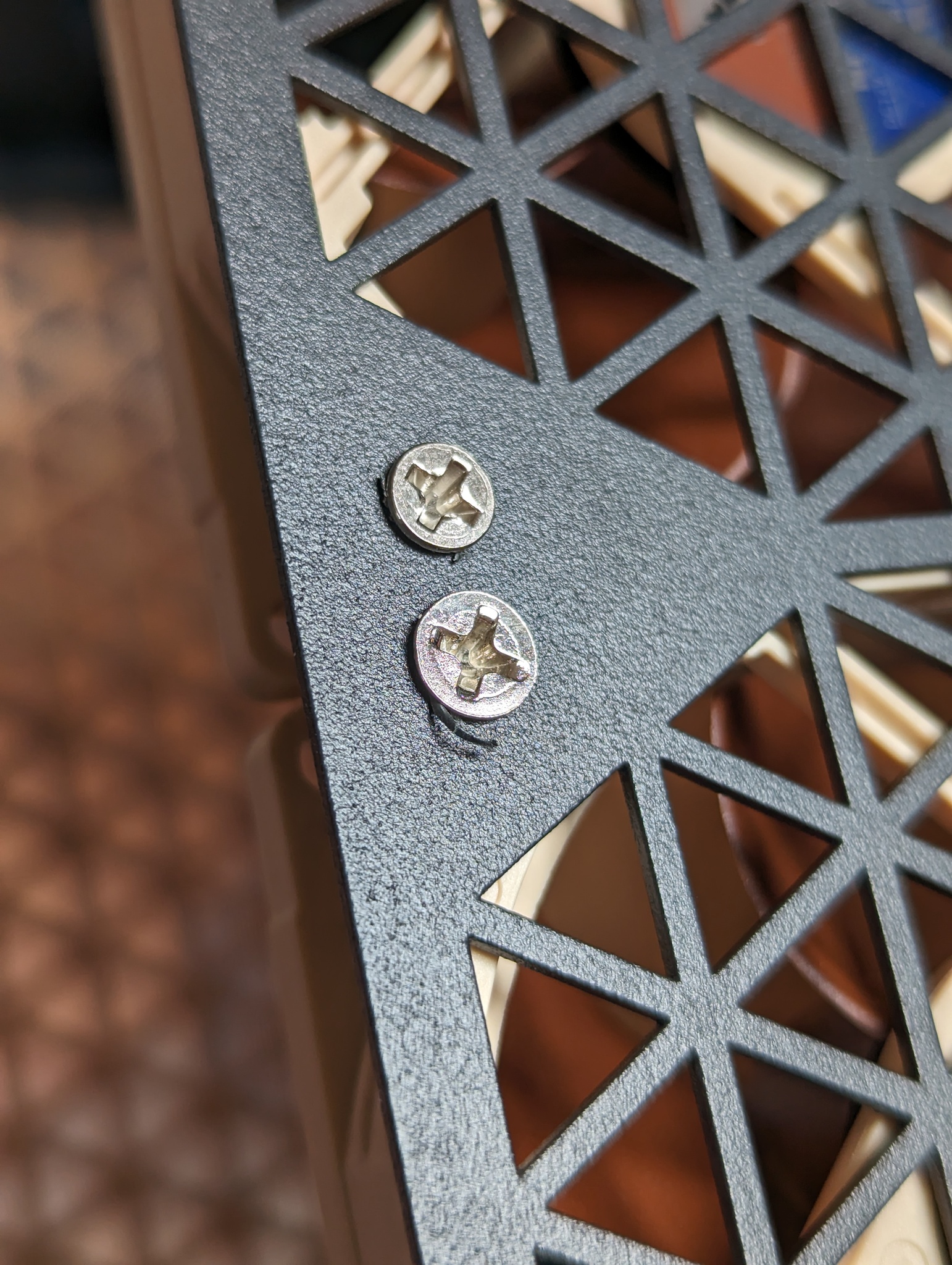
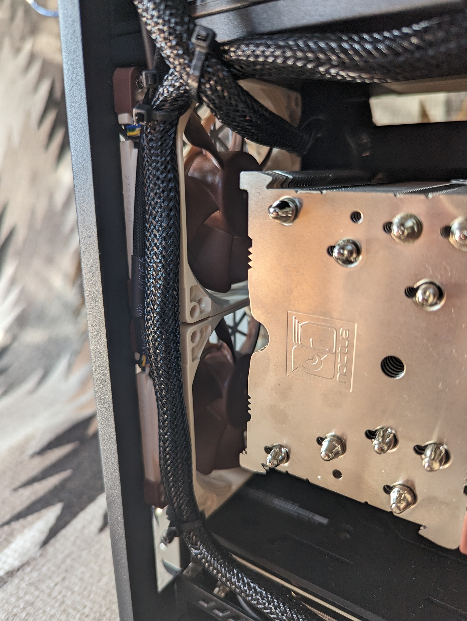
The rear 80mm fan mounting holes are a little tight - not sure if it’s just
the powdercoat, but attaching the rear fans generated a fair few metal chips
that people might want to keep an eye out for, especially if mounting fans
after mounting the motherboard. In addition, the two sets of mounting holes are
quite close together - so close that the silicone dampers on Noctua fans will
actually interfere slightly. On the case-side of the fan, the mounting tension
is enough to pull them in line most of the way, but I had to remove them from
the internal side of the fan since otherwise they would not seat nicely.
Possibly a user error, but the front fan rail did deform somewhat after
snugly installing a 140mm fan in the top front of the case. Possibly an
adversarial positioning since this results in the screw being right in the
middle of the cutout, rather than at one of the more supported ends.
Mount deformation on snug fan install
This isn’t a flaw of the case per se, but be warned that the tolerances for
front fans with a GPU mounted is extremely tight! Even with one of the
smallest GPUs I could find, the fit was so close I had to remove the
silicone dampers on the fan in order to gain the extra fraction of a mm needed
for it to fit cleanly. Looking at it the other way though, this case is
exactly as big as it needs to be in this dimension.
Dust filters
As someone who lives around a lot of pet hair and general dander, dust filters
are pretty crucial on any computer equipment to at least try and keep the
inside clean. Unfortunately the Aski 2 doesn’t come with any, but I was able to
cobble some reasonable ones together using some parts off McMaster (cheaper
sources almost certainly exist). Namely,
If doing this again I might opt for a smaller mesh, though you still want
it to be fairly open so you don’t restrict flow. The 61x61 mesh on McM is
also a 50%+ open area option, so that’s probably a good bet.
The nylon mesh I purchased had no colourant, which made it a little conspicuous
as a filter material out of the box. This was especially true for the PSU
intake, which doesn’t completely fill the top panel (and if I made it
oversized, it would have to have a cutout for the power button).
To make the mesh blend in better, the first thing I did was dye it black.
Dyeing nylon is slightly involved in that you need to use an acid dye. I opted
for the Jet Black (639) from Jacquard dyes, which was readily available, with
citric acid to achieve the necessary pH. Using a cheap baking tray as a vessel
to avoid contaminating food use containers (if you do this, ensure the tray
does not have a non-stick coating that will off-gas hazardous chemicals if
heated directly) I dissolved the dye, soaked some pre-cut sheets of mesh in
the dye solution, added citric acid solution, and then brought to a boil and
let sit for thirty minutes while agitating. Note that getting the temperature
up to boiling is critical for the dyeing process to work - I had to cover the
pan with a metal sheet as a lid to keep heat from escaping.
With the mesh dyed, the previously visible edge of the filter material now
blends pretty seamlessly with the dark powder coat on the chassis.
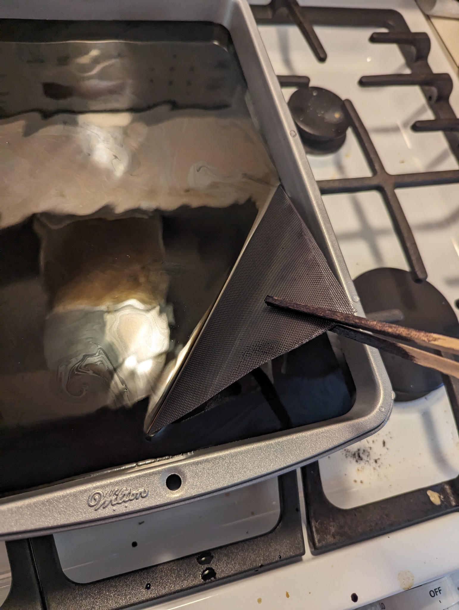
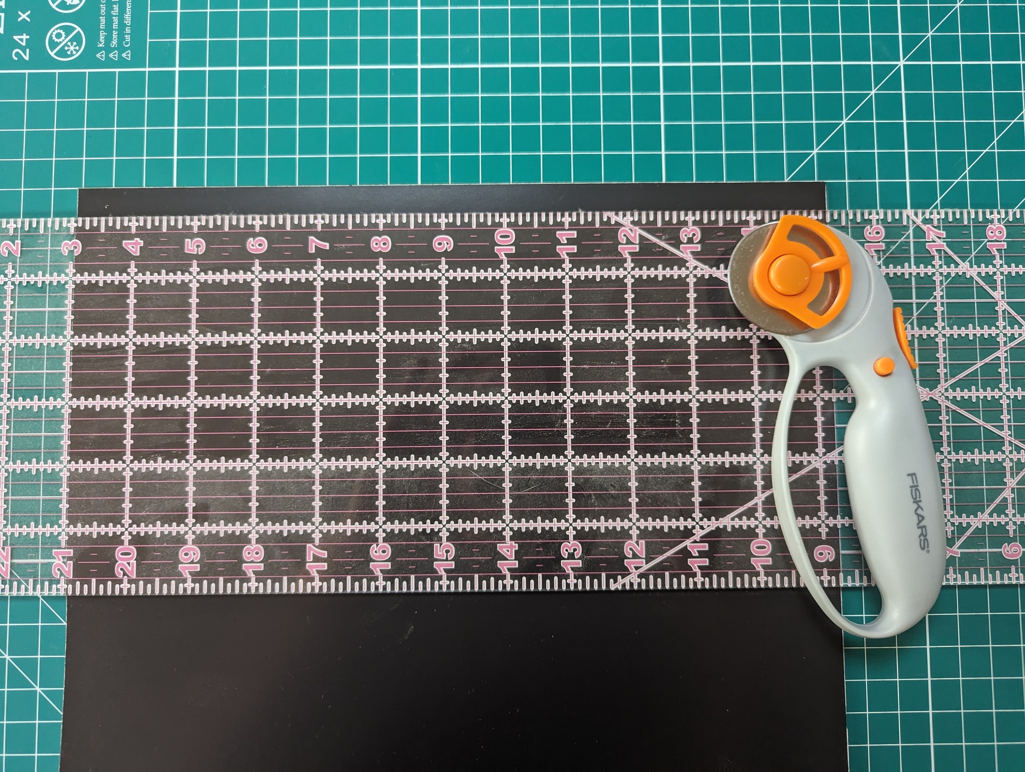
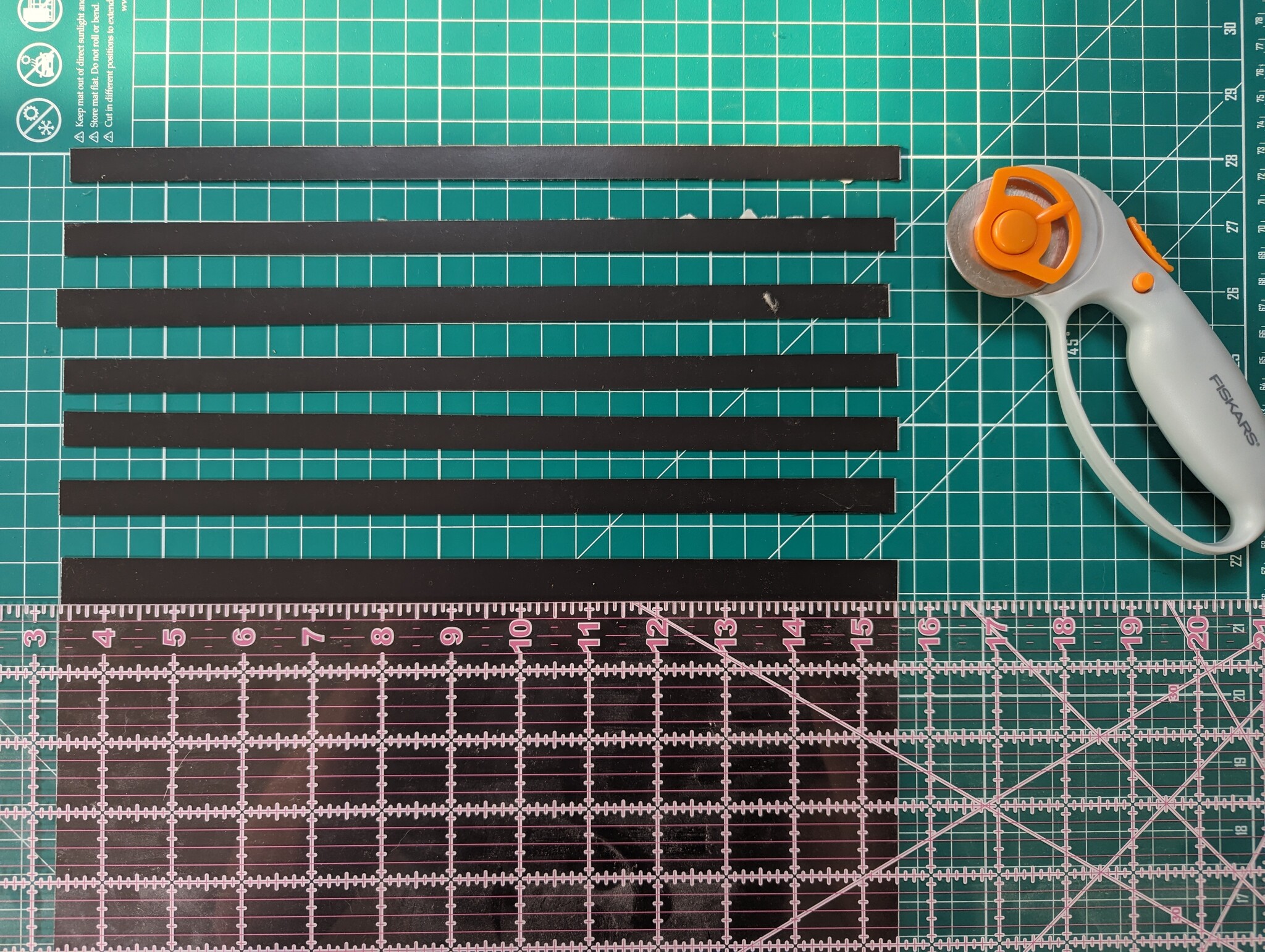
Next, I cut the magnetic sheet into 1cm wide strips using a rotary fabric
cutter, and then slipped them onto the bare case chassis around the
apertures I intended to put dust covers on (all of the ones that will be
intakes). I then cut them down to size lengthwise by eye (cut one then layer it
on the other to ensure they are consistent) then used them as a yardstick to
measure out the nylon mesh, which I again cut using the rotary fabric cutter.
Conveniently the mesh has a built in grid to make sure you cut it square; I
found that cutting it slightly large then intentionally peeling off one edge
strip at a time allowed fine tuning the size easily, after which you can use a
ruler and the cutter to trim the loose ends. I also recommend sizing the mesh
patch slightly narrower than the full width of the case, just so that you have
some wiggle room to pull it taut over the apertures with the magnets.
The adhesive on the back of the magnetic sheet I purchased is strong enough to
tack the filter mesh in place, but unfortunately isn’t enough to keep it there
long term, especially for the bottom intake which has gravity working against
it. To reinforce the bond, I lay a bead of black RTV silicone adhesive
(Permatex 81158) along
the top of each interface and smoothed it into the mesh with a playing card.
Once cured, any excess silicone was trimmed with a pair of scissors. With the
additional adhesive, the filters now feel like they should hold up pretty well
to light abuse.
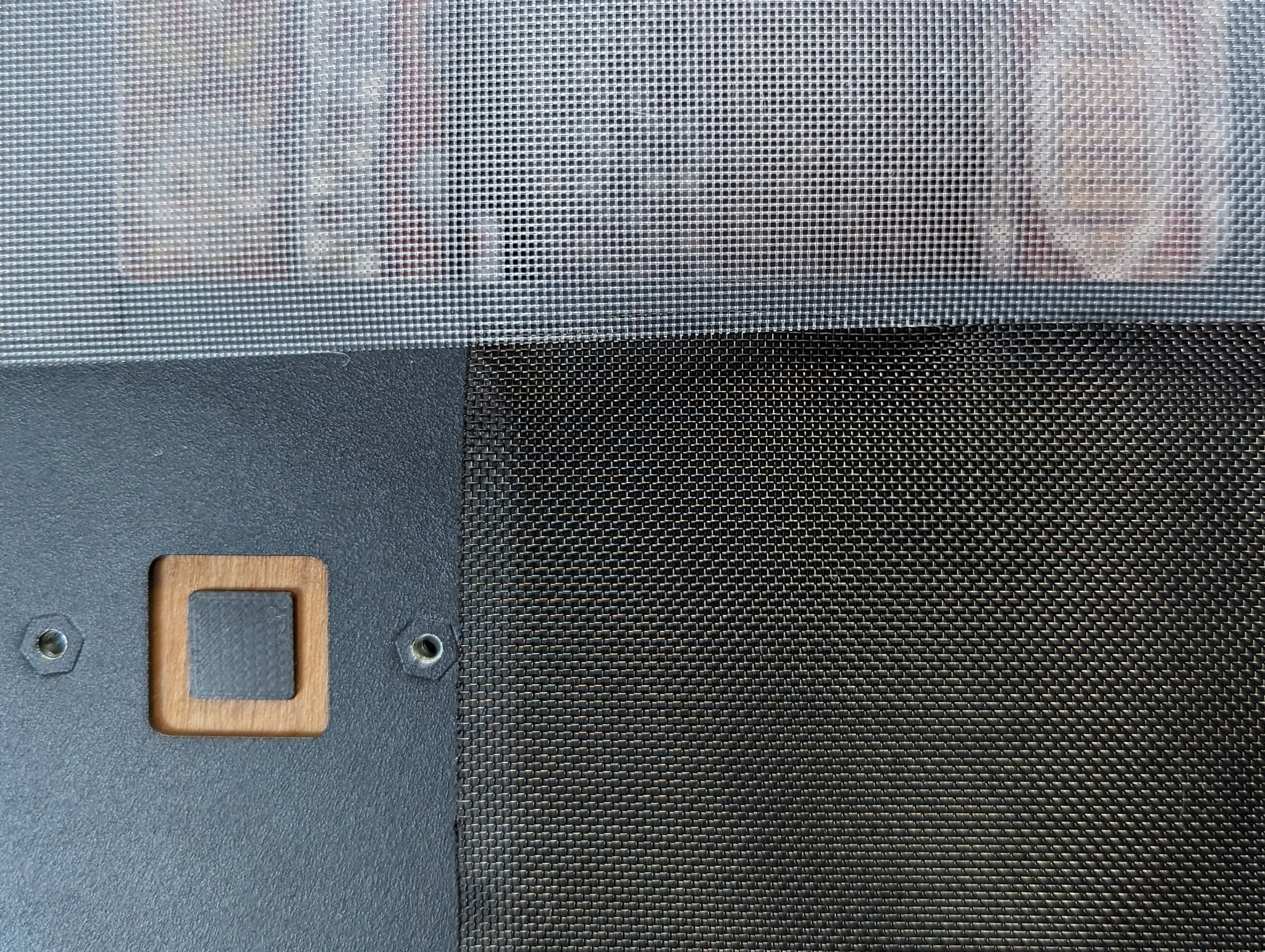
Note that on the front of the case, the combined thickness of the fan screws
and magnet is too much for the front panel to seat comfortably. To get around
this, I notched out the filter on that side to ensure a clean fit. Likewise, on
the bottom intake, I notched the filter in around the four feet, and on the top
intake narrowed one edge so that it can extend between the two attachment
points for the top panel.
I’m quite pleased by how the filters turned out, especially with the black
dye. In addition to blocking dust, the dark filters also help to hide the fans
behind the front grille, leading to a nice clean look for the front of the
case.
Build Process
Small cases generally require a fairly specific installation order for things
to fit, and this one is no exception. I found it worked best to go in this
order:
Assemble the CPU, cooler, memory and SSD to the motherboard.
Fit the motherboard into the case. I used M3x12 button head screws with
nylon washers.
Attach the auxiliary CPU power cable to the motherboard while it is still
accessible.
Install the GPU to the motherboard.
Connect the power button to the motherboard. I chose to route it along the
back side of the motherboard.
Install the rear exhaust 80mm fans. I routed the cables on the top side, away
from the motherboard. Both cables were connected to a splitter and then to
the motherboard.
Install the power supply, plug in the other side of the aux CPU power cable,
and install the primary ATX power cable.
Install the front fans. I found that I had to remove the silicone dampers
in order to gain the extra mm of clearance needed to get them past the GPU.
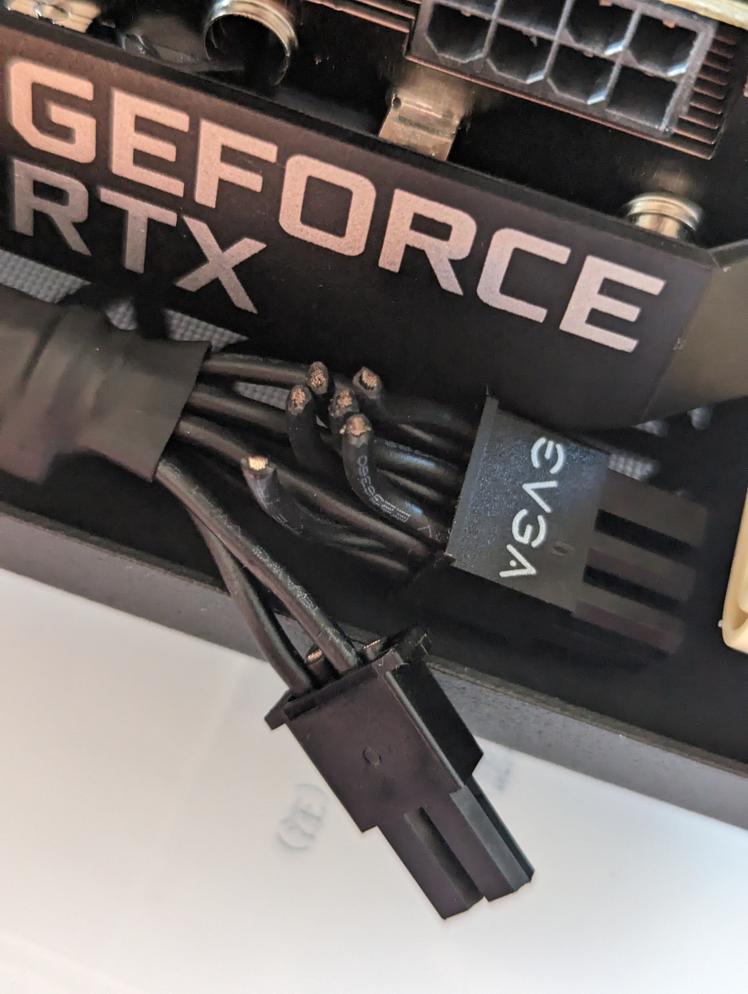
Install the GPU aux power cable. I chose to clip off the daisy chained
connector for a cleaner fit. Ensure that if you do this you trim it very
close to the connector to minimize risk of shorts (shorter than the example
image).
Cable manage the GPU aux power and rear fan cables along the back of the
case using the intake mounting holes of the 80mm fans as binding posts.
System Performance
This case is about 1/7th the volume of my old PC, and I was curious to see how
much raw CPU performance I was giving up, as well as just whether the very
small noctua cooler would be able to keep up with the amount of power thrown
off by the i9-13900K.
To generate a realistic load for the work I usually do, I used a compile of the
6.1 Linux kernel as a benchmark. The system was initially run ouside the case
on my desk, with unrestricted airflow, and only the onboard CPU cooler fan for
air movement. Here are the results for that, along with reference results from
my old desktop and my current laptop:
These results are honestly pretty shocking. The i9 is hot on the heels of the
Threadripper, despite its $600 MSRP being only one quarter of the Threadripper’s
$2400. I expected much more of a margin here. The Threadripper obviously has
other advantages (ECC memory, more memory channels, dramatically more PCIe
lanes, etc) but for this application it’s clear that the i9 blows it out of the
water. Of course, both desktops completely outclass my laptop, which despite
also being a modern CPU SKU can only hit about 35W of continuous package power
with its fitted thermal solution.
Speaking of thermal solutions, the Noctua NH-U9S is rated by Noctua as ‘medium
turbo/overclocking headroom’ for the i9-13900k, and I think that’s a pretty
accurate assessment. The CPU very quickly hit 100°C package temp, and throttled
the P-cores back from about 5.4GHz to about 4.9GHz by the end of the build,
remaining at about 100°C the entire time. By way of comparison, the
Threadripper with a NH-U14S TR4-SP3 sat at at (comparatively) cool 76°C and
4.3GHz all core clocks for the duration of the run.
Cooler Mod
To see if I could eke some more performance out of the NH-U9S, I browsed
Digikey for alternate 92mm fans that might be able to push more air. The best
replacement seemed to be the
Delta AFC0912D-AF00,
which offers much higher numbers than the Noctua across the board:
                    Noctua NF-A9        Delta AFC0912D-AF00
Airflow             1.315 m³/min        2.87 m³/min
Static Pressure     2.28 mmH₂0          13.35 mmH₂0
Acoustic Noise      22.8 db(A)          53.0 dB(A)
Power               1.2 W               9 W
Rated RPM           2000                4800
Note that that includes noise, and this fan is decidedly more of a
‘server-class’ sound than the Noctua fans. I crimped a standard PC fan header
onto the Delta fan, attached it to the cooler tower using the Noctua mounting
clips, and re-ran the compile:
The additional airflow does actually manage to boost the P-core clocks by
300MHz or so, which certainly isn’t nothing. The package temp is also
marginally lower, though still above the 85°C usually used as a cutoff
for non-industrial silicon operating ranges. However, it comes at a significant
noise cost. I don’t have a decibel meter to verify, but subjectively the fan is
distractingly loud. 10dB is approximately a doubling of perceived loudness, so
the thirty decibel rated difference between the fans suggests the Delta is 8x
is loud as the Noctua. For the 4-5% increase in performance, this modification
probably isn’t worth it given the design target of the PC.
Case Airflow
With a baseline for how the system performs in open air, I then installed it
into the case along with all of the auxiliary fans and re-ran the benchmark.
For these runs, the system is back to using the stock Noctua NF-A9 fan since
that’s what I will likely run in the system going forward.
The result was actually a little faster, presumably because of the additional
four fans channeling air around the system.
The VRM on this motherboard is working pretty hard to feed the CPU, and has a
relatively small heat sink that gets quite hot. Annoyingly, despite being
present in the BIOS that temperature control doesn’t seem to be exposed by
lm-sensors, but I’d wager it’s also happier with the guided
case airflow, as are the memory DIMMs. At idle, all temperature zones measure
around 40°C.
Overall
I’m very charmed by this case. I think it looks very attractive as a desk
piece, is well built, and the internal design makes it surprisingly easy to
work with despite the small size. Being able to fit a 2U PCIe card in there
without a riser is also a very nice design achievement. The patterning on the
front allows for pretty good airflow, even with the added dust filters. If I
were to complain about anything, it would be that there are no filters
included, but considering the space to work with it’s understandable.
The complete lack of any front panel I/O could also be a downside depending on
your preferences, but at least for me I’m alright trading it for a clean
design.
This post contains writeups and some code samples for solving each of
the puzzles from the
DC29 HHV Challenge
roughly organized by complexity.
Many thanks to the
HHV members that ran the CTF
(rehr, wintermute, diogt and any others)!
Plenty of spoilers follow!
Welcome
Backup Logs
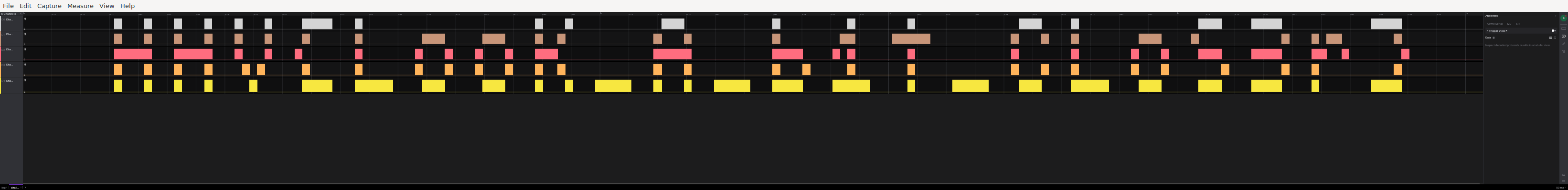
For part a, we need to take the long view. Shrinking the interface size
on Logic makes this a bit easier:
The Big Picture
For part b, careful examination of the clock signals (or blindly adding uart
decoders to every signal) reveals that one of our
channels actually transmits UART data for part of the trace.
Secret board
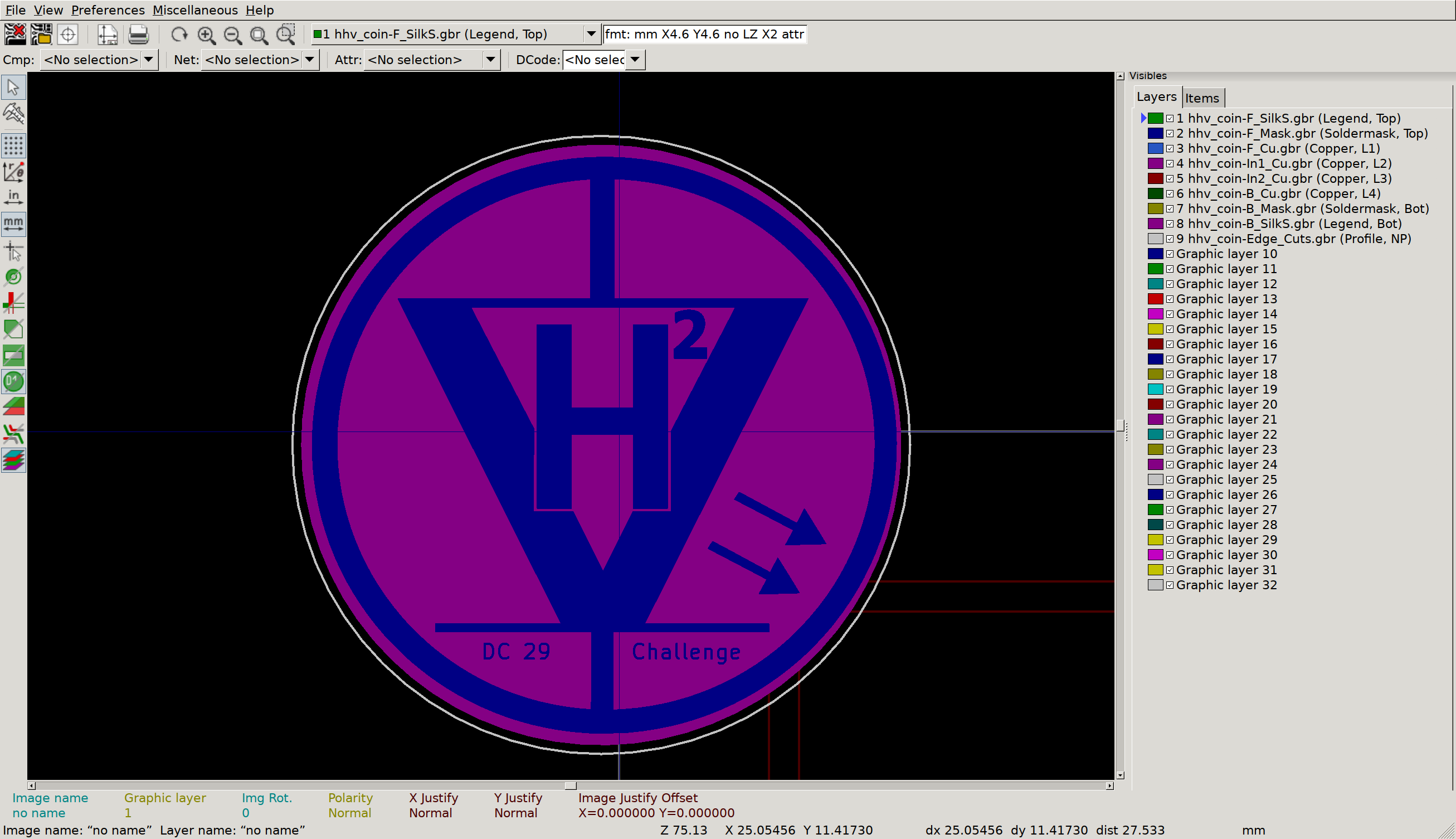
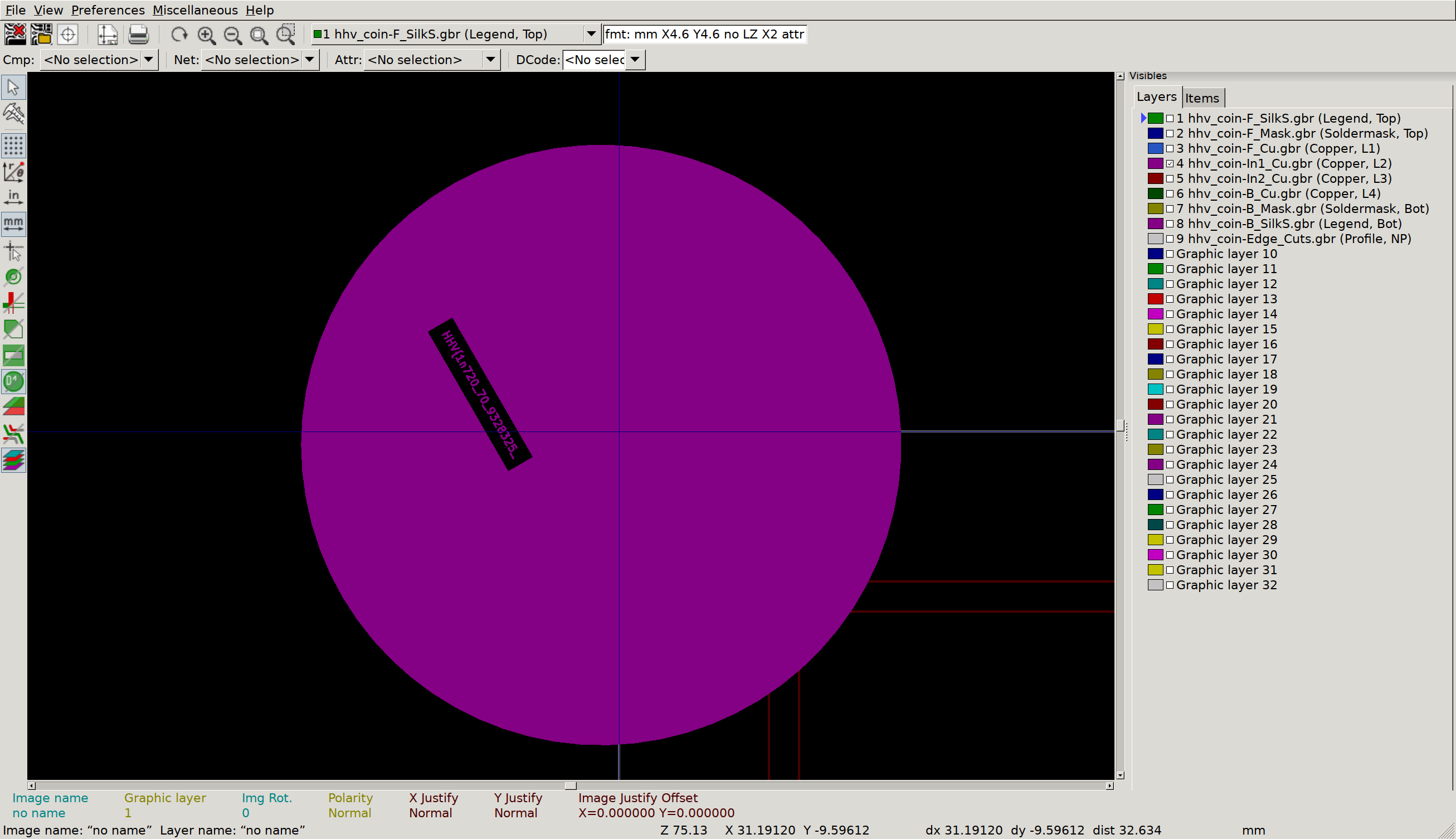
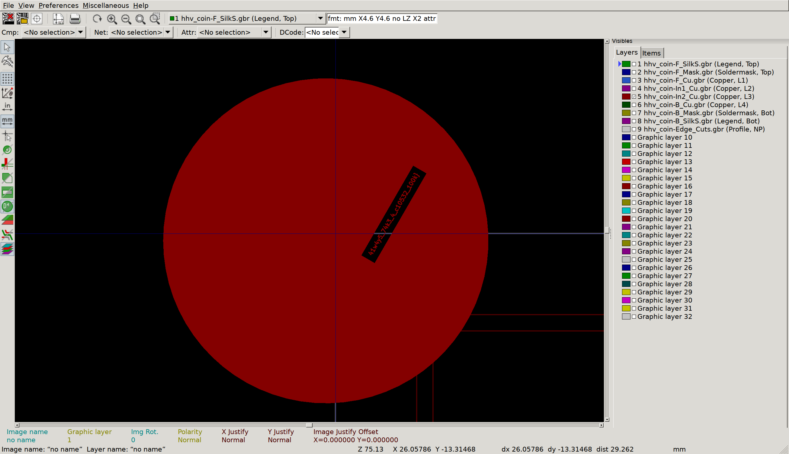
The filenames in the zip are all .gbr, or Gerber files for PCB fabrication data.
Opening them in a
viewer (e.g. gerbview or gerbv) reveals a nice little badge
What a nice badge
But what’s this, on the inner copper layers?
Inner Copper 1
Inner Copper 2
Circuit Cave
This is the way
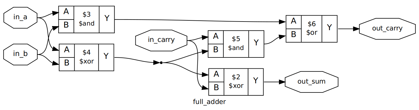
I’d never seen a .circ file, and wasn’t sure exactly how to open it, so I just
took a peek at the start to see what sort of format we were dealing with.
Luckily, it comes with a clue!
ross@mjolnir:/h/r/Downloads$ head challenge.circ
<?xml version="1.0" encoding="UTF-8" standalone="no"?><projectsource="2.7.1"version="1.0">
This file is intended to be loaded by Logisim (http://www.cburch.com/logisim/).
<libdesc="#Wiring"name="0"/><libdesc="#Gates"name="1"/><libdesc="#Plexers"name="2"/><libdesc="#Arithmetic"name="3"/><libdesc="#Memory"name="4"><toolname="ROM">
After installing logisim from apt, we are greeted with a circuit that will
shuffle out some obfuscated data on some seven segment displays. Presumably,
this data is ascii for our flag. Writing down all the numbers by hand
seems burdensome, but if you open the Similation -> Logging window you can add
the output of the decoder circuit, and change the radix to 16 to record the hex
value every time it changes. Combine this with the log to file option and a
method to convert hex as ascii, and you have your flag. Or… close to your
flag. It seems that we only actually want every 8th output digit, or whatever
is loaded when the Counter(240, 350) signal wraps to zero (when the decimal
point is lit).
To speed things up, I recommend changing the Simulate -> Tick Frequency value to
something zippier than the default 1Hz.
No, this is the way
I’m a big fan
of verilator! To get the flag here, I made one small addition to
the tick code in the testbench:
tb->i_clk =0;
tb->eval();
// If the module has flagged the output data is valid, print that
// character to stdout
if (tb->o_out) {
printf("%c", tb->o_data);
}
if (tfp) {
tfp->dump(tickcount *10+5);
tfp->flush();
}
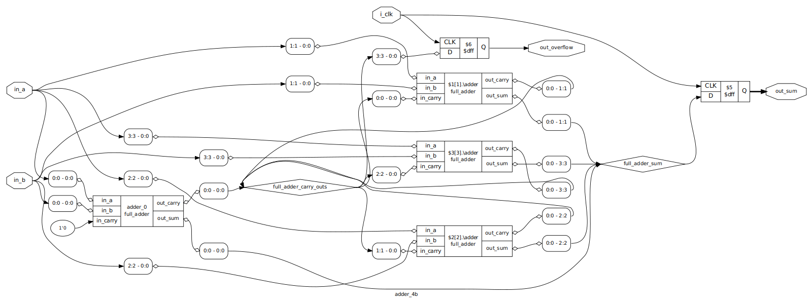
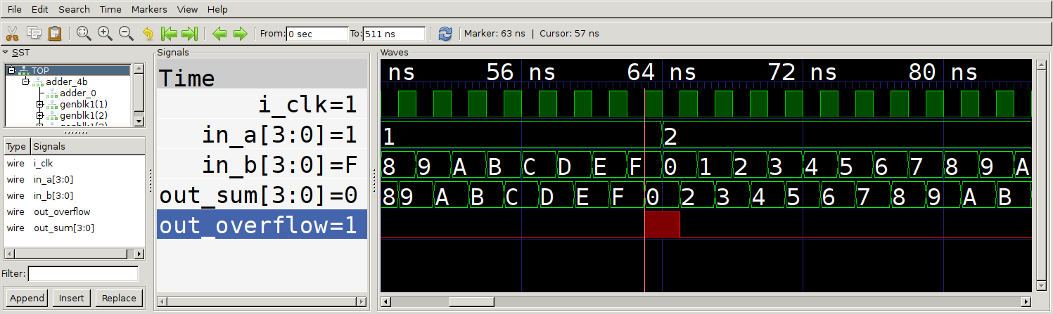
The only true way
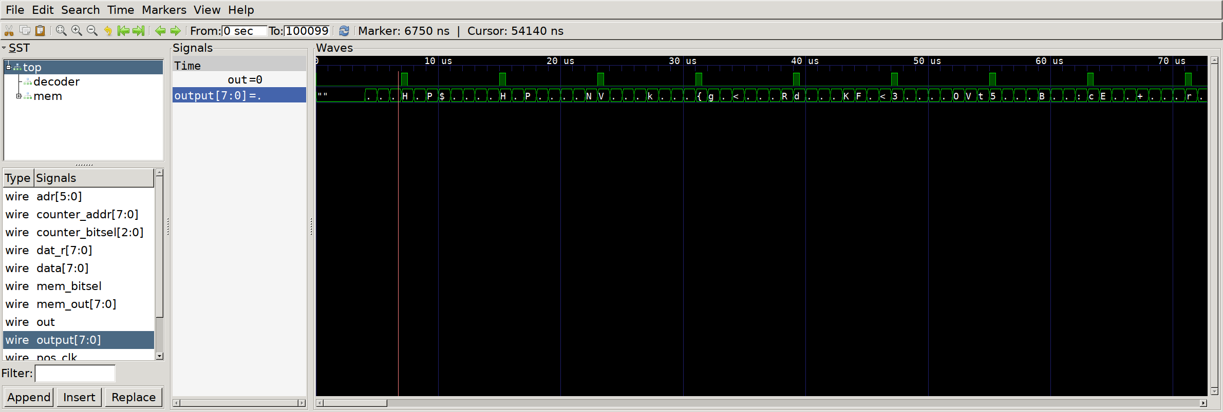
This stage is similar, but uses nmigen instead of verilog. I’ve seen some
nmigen stuff before, but haven’t stuck much of a toe in since I feel I need to
thoroughly understand Verilog first. I couldn’t immediately spot a simple way
to log data during the similation, so I did this the dumb way - opened up the
trace in gtkwave and manually transcribed the data. Sometimes simple works!
GTKwave to the rescue
Biggest problem I had here was getting nmigen to run properly - there seemed to
be some sort of dependency ordering issue, where if I installed nmigen and then
nmigen_soc, it would downgrade nmigen to a version that doesn’t have similation.
Installing nmigen_soc, then reinstalling nmigen again seemed to fix the
problem for my virualenv.
Serial Swamp
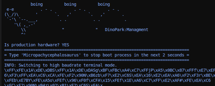
Debuggin Interface
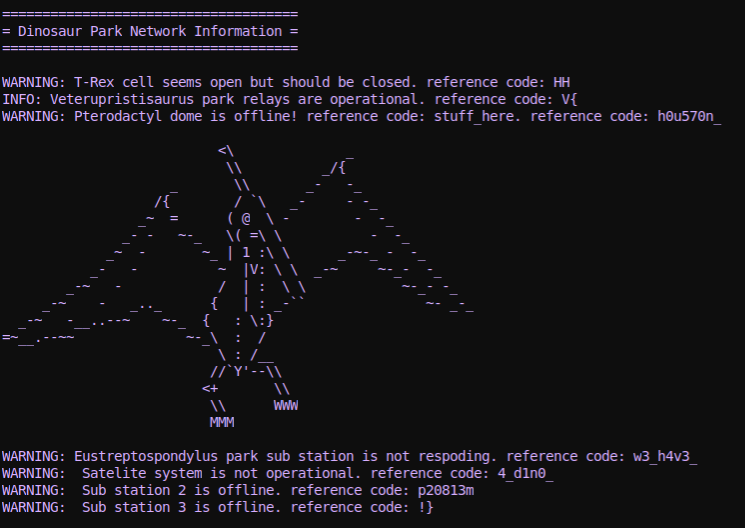
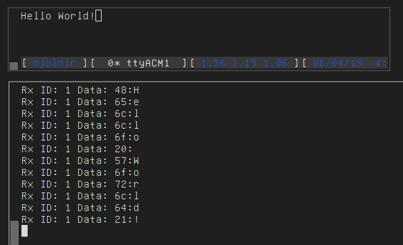
Looks like UART at first glance. Add a decoder with a nice default 9600 baud
and we see a cute dinosaur in our console output:
Micropachycephalosaurus
Near the end we see a note that we are switching to fast uart to continue.
Add a second decoder with the mildly zippier 115200 baudrate and we can see the
rest of our boot prompt, including flag:
Pterodactyl dome
Lost Record
Wasn’t sure immediately what to make of this one, but googling our signal
names (BCK, LRCLK, DOUT) suggests that this is an i2s (audio) interface with 2
channels. Counting our clock cycles, it looks like we have 32 bits per sample,
and scanning through some of our early data samples it seems likely that
the values are signed, encoded as 2’s complement (instead of toggling between
min and max amplitude very quickly).
First step here is to reconstruct the audio, so let’s add an i2s analyzer in
Logic and export the data as a CSV. We can then use python to scarf the data
and emit a flat binary file with packed sample data, like so:
importcsvimportsysimportstructclassSample(object):
def __init__(self, time, channel, data):
self.time = time
self.channel = channel
self.data = data
# Read the CSV data
samples = []
withopen(sys.argv[1]) as f:
reader = csv.reader(f)
reader.next() # Skip headerfor row in reader:
try:
samples.append(Sample(
float(row[2]), # Timestampint(row[5]), # Channel (L/R)int(row[6]) # Sample data
))
exceptException, e:
print e
print row
# Calculate sample rate
time_start = samples[0].time
time_end = samples[-1].time
sample_time = time_end - time_start
sample_count =len(samples)
samples_per_sec = sample_count / sample_time /2print"Sample rate: %f"% samples_per_sec
# Create an array of data for each channel
ch0 = []
ch1 = []
for sample in samples:
if sample.channel ==0:
ch0.append(sample.data)
if sample.channel ==1:
ch1.append(sample.data)
# Interleave the data and pack down into a filewithopen('out.stereo.bin', 'wb') as f:
for pair inzip(ch0, ch1):
f.write(struct.pack('ii', pair[0], pair[1]))
We can test that the audio sounds right by playing it raw:
aplay -f S32_LE -c 2 -r 44100 out.stereo.bin
My god! They’re coming back! But that doesn’t seem to be the trick. Let’s load
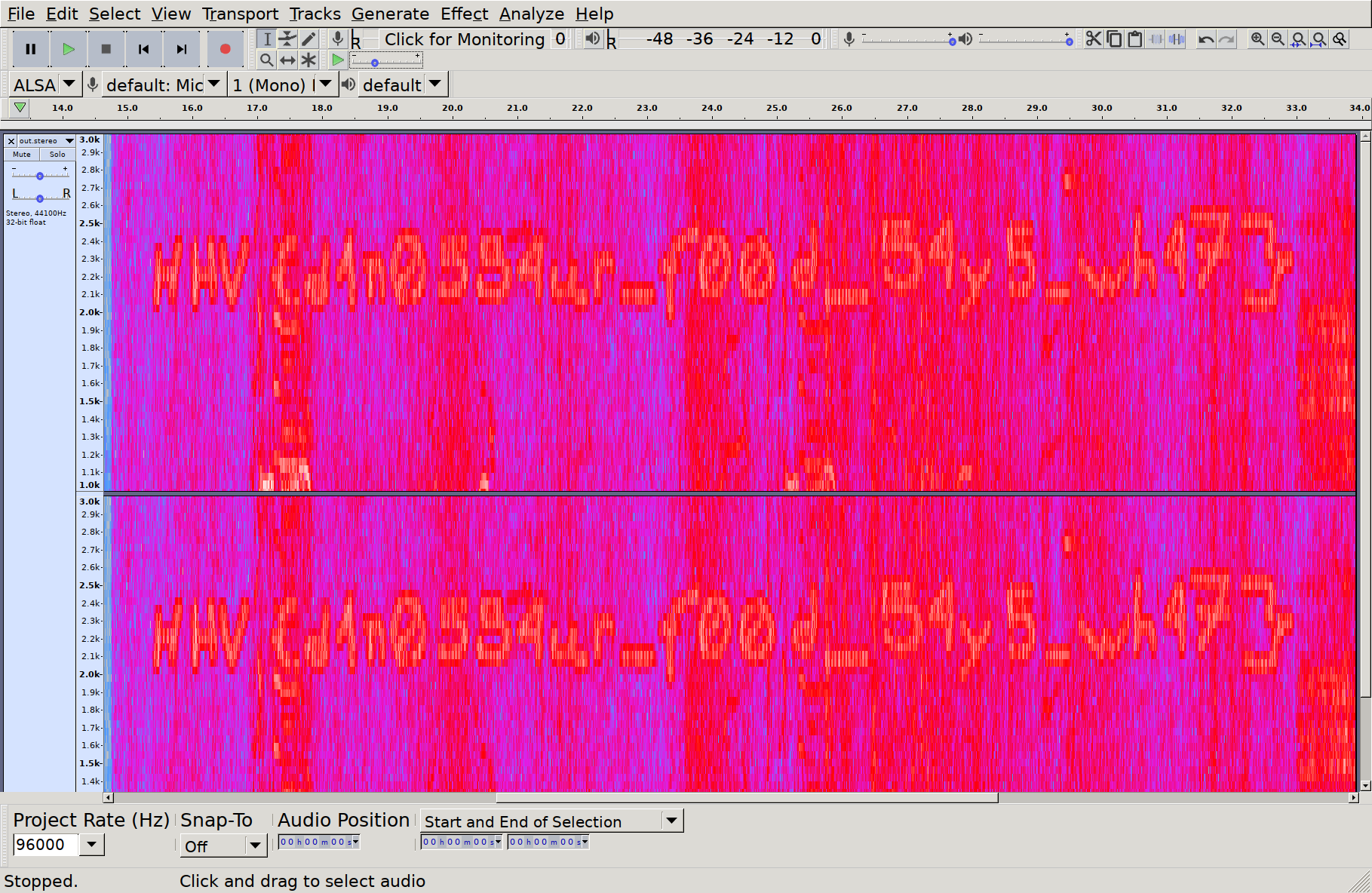
this audio into audacity so that we can poke around a bit -
A fun steganographic technique with audio files is embedding pictures in the
Spectrogram
of the track. Let’s enable spectrogram view and zoom on in to that final
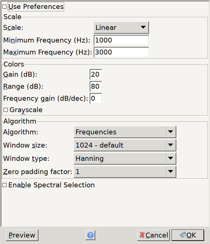
segment:
Suggested settings for spectrogram view
Who drew this here
Lab Control
This one took some doing, mostly due to the sheer size of the datasheet for
this chip, and the lack of a clear transaction process overview. But, first
things first, we need to make sense of this data - scanning the trace in Logic,
it looks like some bog standard SPI transactions. From the chip datasheet, it
looks like spi transactions consist of an address and Read/~Write bit, followed
by the read/written data. So, let’s decode the data in Logic and export a CSV
we can run through some analysis. The output of our export will look like the
following:
First things first is to load this data into a programming language where we
can mess around a bit, so here’s a quick and dirty loader in C++:
// A 'transaction' begins when ~CS goes low, ends when it goes high.
// Multiple bytes could be transferred per transaction.
struct Txn {
std::vector<uint8_t> mosi;
std::vector<uint8_t> miso;
};
// ...
// Load input file
constchar*filename = argv[1];
std::fstream fstream_in;
fstream_in.open(filename, std::ios::in);
if (!fstream_in.is_open()) {
fprintf(stderr, "Failed to open %s\n", filename);
return-1;
}
// Split each line, and extract our important fields
std::string line;
std::vector<Txn> txns;
bool is_in_txn =false;
Txn active_txn;
while (std::getline(fstream_in, line)) {
std::stringstream row_ss(line);
std::string field;
std::vector<std::string> fields;
while (std::getline(row_ss, field, ',')) {
fields.emplace_back(field);
}
if (fields[1] =="\"enable\"") {
is_in_txn =true;
} elseif (fields[1] =="\"result\"") {
active_txn.mosi.emplace_back(strtoll(fields[4].c_str(), nullptr, 16));
active_txn.miso.emplace_back(strtoll(fields[5].c_str(), nullptr, 16));
} elseif (fields[1] =="\"disable\"") {
txns.emplace_back(active_txn);
active_txn = {};
} else {
fprintf(stderr, "Unknown op '%s'\n", fields[1].c_str());
}
}
Once we have all the transactions, each of which starts with an address, we can
scan through for addresses that are ‘interesting’. First one that looks
promising to me is FIFODataReg - if there’s data, it’s going to be passing
through there. So what happens if we print all the contiguous reads/writes to
that register?
bool last_was_fifo_read =false;
for (auto&txn : txns) {
// MSB controls read/write
constbool is_read = txn.mosi[0] & (1<<7);
// Address is left shifted one bit just to trip you up
const uint8_t addr = (txn.mosi[0] &0x7F) >>1;
// Contiguous read from FIFO?
if (is_read && addr ==0x09) {
if (!last_was_fifo_read) {
printf("\n[RD] ");
}
printf("%02x", txn.miso[1]);
last_was_fifo_read =true;
} else {
if (last_was_fifo_read) {
printf("\n");
}
last_was_fifo_read =false;
}
// Contiguous write to FIFO?
// [...]
If we run this, we see some interesting long strings of hex data:
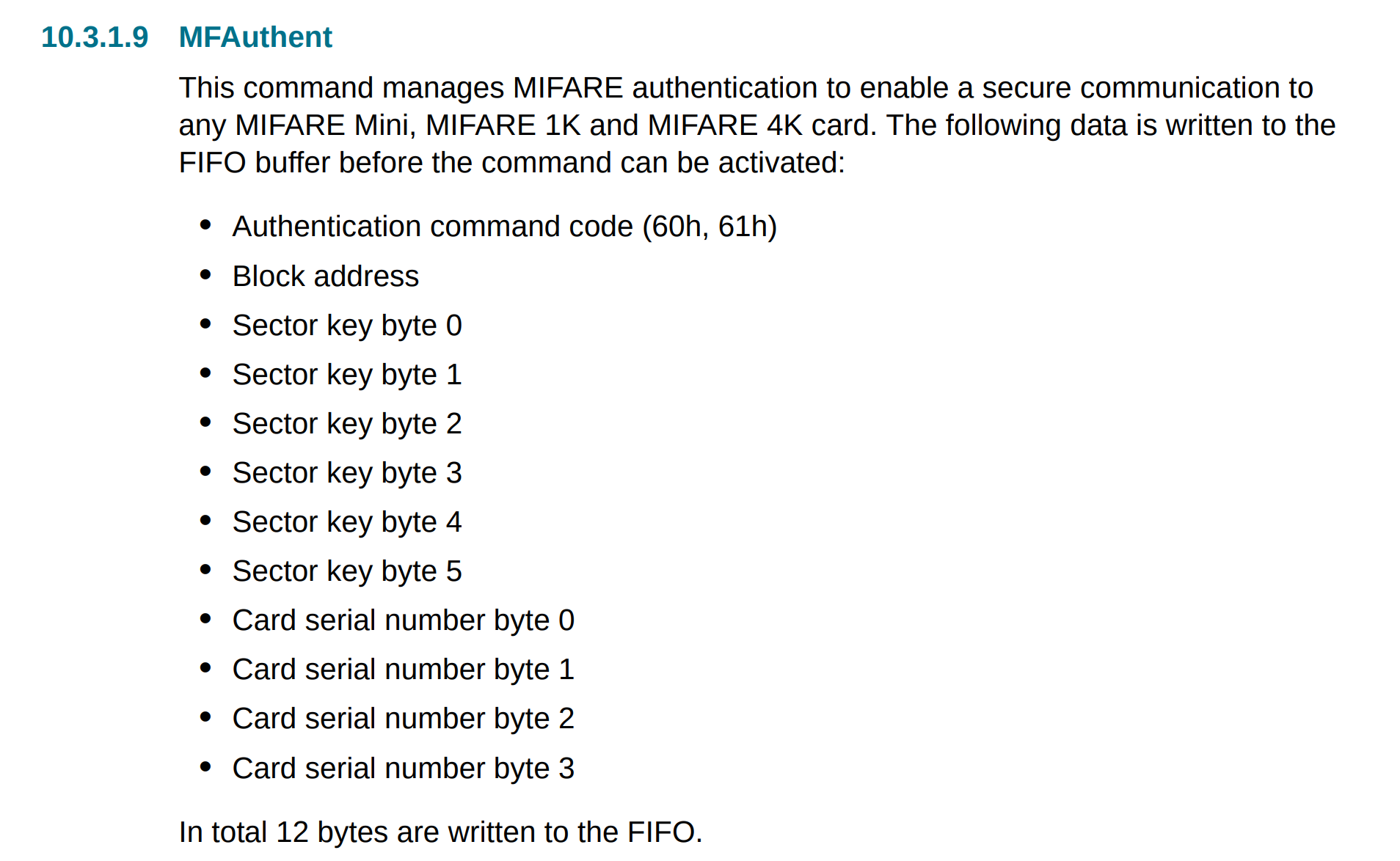
MFAuthent - if we search the datasheet for this, we get a hit well over a
hundred pages in:
MFAuthent packet structure
If we break down the data written to the FIFO right before this command, it
looks like it matches nicely:
60              # Authentication command
08              # Block address
f02d53fda4a7    # Sector key
8634cd1f        # Card serial number (Uid)
If we combine the data from this write (UID and sector key) with the data from
the Transceive calls that happen right after it, we have all the data we need
for our key:
This is a fun one. We have a trace with a clock, MOSI, reset and ‘DC’
line, and know that we are talking to a display controller. These controllers
tend to have Data vs Control modes, so this is likely what our DC signal
represents. In order to attack this, we will want to export the commands sent
to the LCD, and then run them through a little simulator to recreate the pixel
state that the display would have. First step is to get the data out of Logic
and into something more parsable. To do this, I added two SPI decoders - both
use CLK, MOSI and DC as the serial clock / data / chip select lines, but one of
them has CS set as active low and the other has it active high. This way, one
will only trigger for data mode transfers and the other only triggers for
control mode transfers. If we name these decoders nicely and export, we get
data like so:
Now, let’s load this up and see what’s involved in replaying this data. First,
some boilerplate:
struct Packet {
enum Type {
COMMAND,
DATA,
};
Type type;
uint8_t data;
};
// [...]
// Parse file
constchar*filename = argv[1];
std::fstream fstream_in;
fstream_in.open(filename, std::ios::in);
if (!fstream_in.is_open()) {
fprintf(stderr, "Failed to open %s\n", filename);
return-1;
}
std::string line;
std::deque<Packet> packets;
while (std::getline(fstream_in, line)) {
std::string::size_type comma_pos = line.find(",");
std::string type = line.substr(0, comma_pos);
std::string value_str = line.substr(comma_pos +1);
Packet p;
p.type = type =="\"data\""? Packet::Type::DATA : Packet::Type::COMMAND;
p.data = strtol(value_str.c_str(), nullptr, 16);
packets.emplace_back(p);
}
We now have a queue of command and data packets. From here, we just need to
peel off the first command, see how many data bytes we need to associate with
it, update the state of our fake LCD, and rinse and repeat. In fact, it turns
out we can ignore most of the setup commands, though it’s useful to note that
the LCD is programmed in 16-bit data mode, where each pixel is RGB565. Skipping
through the rest of the commands from the datasheet, we come across three that
we definitely want to implement - the Row/Column window select, and the RAMWR
commands. The LCD controller in question does not allow you to addresss the
entire memory space at once, instead you have to define an X region xs (x
start) to xe (x end), and similarly a Y region, into which the RAMWR function
will write. So, let’s do some accounting for these in a little loop:
// Cannot understand why STL containers don't include a method for this
auto next_packet = [&]() -> Packet {
auto p = packets.front();
packets.pop_front();
return p;
};
// Row/column window, and current pixel write address
uint16_t xs =0, xe =0xef;
uint16_t ys =0, ye =0x13f;
uint16_t x_addr = xs;
uint16_t y_addr = ys;
// State machine
while (packets.size()) {
// Take first packet
auto packet = next_packet();
// Ignore unexpected data packets
if (packet.type == Packet::Type::DATA) {
fprintf(stderr, "Unexpected data packet %02x\n", packet.data);
continue;
}
// Switch next packet command
switch (Command(packet.data)) {
case Command::COL_ADDR_SET: {
// Consume 4 data packets
auto xs15_8 = next_packet();
auto xs7_0 = next_packet();
auto xe15_8 = next_packet();
auto xe7_0 = next_packet();
xs = xs15_8.data <<8| xs7_0.data;
xe = xe15_8.data <<8| xe7_0.data;
x_addr = xs;
fprintf(stderr, "xs: %4d, xe: %4d\n", xs, xe);
} break;
case Command::ROW_ADDR_SET: {
// Consume 4 data packets
auto ys15_8 = next_packet();
auto ys7_0 = next_packet();
auto ye15_8 = next_packet();
auto ye7_0 = next_packet();
ys = ys15_8.data <<8| ys7_0.data;
ye = ye15_8.data <<8| ye7_0.data;
y_addr = ys;
fprintf(stderr, "ys: %4d, ye: %4d\n", ys, ye);
} break;
default: {
fprintf(stderr, "Unhandled command 0x%02x\n", packet.data);
} break;
}
}
Now that we have the row/column data, we need to actually write pixels to those
addresses. We create a buffer to hold our pixel data & some helper tools to
write data, then handle that command type in our loop like we did the row/col
addresses:
// Display is a known size
constint rows =240;
constint cols =320;
static uint8_t pixels[rows * cols *3];
auto write_pixdata = [&](int row, int col, uint16_t data) {
// input data is rgb 565
uint8_t r = (data >>11) &0b11111;
uint8_t g = (data >>5) &0b111111;
uint8_t b = (data >>0) &0b11111;
constint offset = (row * cols + col) *3;
pixels[offset +0] = r;
pixels[offset +1] = g;
pixels[offset +2] = b;
};
// [...]
// Inside our switch statement from above
case Command::RAMWR: {
// Consume as many data packets as we can
int wrote =0;
while (packets.front().type == Packet::Type::DATA) {
// Pop 2 data packets
auto dp0 = next_packet();
auto dp1 = next_packet();
uint16_t dat = dp0.data <<8| dp1.data;
write_pixdata(x_addr, y_addr, dat);
// Handle row/column address increment
x_addr++;
if (x_addr > xe) {
x_addr = xs;
y_addr++;
}
if (y_addr > ye) {
y_addr = ys;
}
wrote++;
}
fprintf(stderr, "Wrote %d pixels\n", wrote);
} break;
This should be enough to regenerate a pixel buffer, but we need a way to see
it. Luckily, openGL makes this relatively straightforward - we can create a
texture, load the pixel data into it, then render it as a flat square using the
following incantations:
// Glut needs a render functin to call; annoyingly can't use a std::function
// so work around by just making key state static
staticint window_w = cols, window_h = rows;
static GLuint gl_texture;
auto gl_display = []() {
glClear(GL_COLOR_BUFFER_BIT | GL_DEPTH_BUFFER_BIT);
// Generic 2d orthographic view
glViewport(0, 0, window_w, window_h);
glPushMatrix();
glOrtho(0, window_w, window_h, 0, -1, +1);
// Render texture as full screen
glBindTexture(GL_TEXTURE_2D, gl_texture);
glEnable(GL_TEXTURE_2D);
glBegin(GL_QUAD_STRIP);
glTexCoord2f(0.0f, 1.0f);
glVertex2f(0, window_h);
glTexCoord2f(0.0f, 0.0f);
glVertex2f(0, 0);
glTexCoord2f(1.0f, 1.0f);
glVertex2f(window_w, window_h);
glTexCoord2f(1.0f, 0.0f);
glVertex2f(window_w, 0);
glEnd();
glDisable(GL_TEXTURE_2D);
glBindTexture(GL_TEXTURE_2D, 0);
glPopMatrix();
glFlush();
glutSwapBuffers();
};
auto gl_resize = [](int w, int h) {
window_w = w;
window_h = h;
};
// Initialize GLUT
glutInit(&argc, argv);
// Create a window to display in
glutInitDisplayMode(GLUT_RGB | GLUT_DOUBLE | GLUT_DEPTH);
glutInitWindowSize(window_w, window_h);
glutInitWindowPosition(0, 0);
glutCreateWindow("Broken Display");
// Set up our render callbacks
glutIdleFunc(gl_display);
glutDisplayFunc(gl_display);
glutReshapeFunc(gl_resize);
// Generate texture using our pixel data
glGenTextures(1, &gl_texture);
glBindTexture(GL_TEXTURE_2D, gl_texture);
glTexImage2D(GL_TEXTURE_2D, 0, GL_RGB, cols, rows, 0, GL_RGB,
GL_UNSIGNED_BYTE, pixels);
glTexParameteri(GL_TEXTURE_2D, GL_TEXTURE_MAG_FILTER, GL_LINEAR);
glTexParameteri(GL_TEXTURE_2D, GL_TEXTURE_MIN_FILTER, GL_LINEAR);
glTexParameteri(GL_TEXTURE_2D, GL_TEXTURE_WRAP_S, GL_CLAMP);
glTexParameteri(GL_TEXTURE_2D, GL_TEXTURE_WRAP_T, GL_CLAMP);
glPixelStorei(GL_UNPACK_ROW_LENGTH, 0);
glBindTexture(gl_texture, 0);
glutMainLoop();
With this, we get a cute little QR code in hacker green. My phone had a hard
time reading this as-is, so I had to screenshot it, open it in GIMP and value
invert the colours to get something it was happier with.
Sun, Aug 23, 2020Companion code for this post available on Github
One of the core design patterns in the arsenal of an FPGA developer is the
finite state machine. Such systems can be small, fast, easy to reason about and
extremely powerful for sequential logic. But there can come a point where a
state machine grows so complex that the hardware implementation starts to
become extremely costly, or perhaps you want to be able to update the behaviour
of a large state machine from an external memory. At such a time, it may
make sense to consider replacing a complex special-purpose state machine with a
highly evolved general purpose state machine - in other words, a CPU.
In this post, we will cover the basic idea of what a soft CPU is, how to
connect a CPU to ROM and RAM using the
Wishbone
bus, how to write firmware for
our custom SoC, how to use interrupts, and how to build our own memory-mapped
IO peripherals. This post will assume some familiarity of Verilog and C++ code;
if readers are less familiar with Verilog I would recommend starting with
this post
that attempts to explain what FPGAs are, and how Verilog can be used to command
them.
Soft CPUs
If one considers the stripped down structure of a CPU, they can start to see how
a CPU is, at its core, simply a state machine - it loads an instruction,
decodes the instruction, performs some operation based on the instruction,
increments the program counter and transitions back to the fetch state. One
could definitely have some fun creating their own minimal CPU with a custom
instruction set, but the level of complexity and tooling that goes into a
performance-competitive CPU is no mean feat. Thus, for someone that wants to
get a system built with minimal reinvention, it makes sense to utilize one of
the increasingly many CPUs available online. There are many to choose from -
this article has a good
rundown of some free options, and even proprietary designs such as the ARM
Cortex-M0 are
available for evaluation.
However, the complexity of integration and licensing headaches are somewhat of
a negative for ARM cores in particular.
For the purposes of this article, we will focus instead on the highly
customizable and increasingly
popular RISC-V ISA, which boasts multiple free implementations targeting
different use cases.
One of the earliest such CPUs. Optimized primarily for small size and high max
frequency, this core has weaker performance per clock cycle numbers than some
other CPUs but is easy to integrate and can fit handily in even some of the
smaller FPGAs on the market.
One of the more unique cores, SERV is a bit-serial architecture - by taking the
tradeoff between clock cycles and design area to the extreme, this CPU
executes on only one bit at a time (instead of on 32 bits at once), reducing
the size of the core to the point that at least 16 cores may be instantiated
on the ICE40LP8K, an FPGA with only 7680 logic elements.
Of the readily available FOSS RISC-V cores, the VexRiscv is certainly the most
configurable. The core itself is written using Spinal HDL, a set of Scala
libraries, which allows for higher level components to be tweaked more readily
than would be possible in straight Verilog.
It can be tuned
all the way from a minimal 500 LUT core with no hardware multiply or interrupt
support all the way up to a 3000 LUT variant with caches, interrupts, branch
prediction and MMU that allows one to run a full Linux core.
Customizing the VexRiscv
Given the customizability of the VexRiscv, and the superior performance per
clock cycle compared to the other options, we will use it as our base for this
project. The downside to customizability is understanding all these
configuration options, so the first thing to do is have a read through some of
the example core generation files, and write our own CPU definition to meet our
needs.
If we take a look at the
demo
folder in the VexRiscv repo, we see a number of templates we can use to base
our core off. We will mostly pull from the GenFull example, and our full
custom configuration and generated CPU file can be found in the repo for this blog post
here.
If we read through our custom
GenVexRiscv.scala,
we can see that the CPU is constructed of various plugins. Most are named
in a fairly self-explanatory way, or do not require much modification, so we
will touch on only some of them directly here. The first is our ibus, or
instruction data bus plugin:
// We need an instruction data bus on the CPU. This bus is separate
// from the data bus for performance reasons, and here we will
// instantiate the cached version of this plugin, which is a
// significant performance improvement on a non-cached implementation
newIBusCachedPlugin(// We want to be able to set the reset address in verilog later, so
// leave it null here
resetVector =null,// Conditional branches are speculatively executed.
// There is no tracking of whether a branch is more likely to be
// executed or not
prediction =STATIC,// Include a 4KiB instruction cache
config =InstructionCacheConfig(
cacheSize =4096,
bytePerLine =32,
wayCount =1,
addressWidth =32,
cpuDataWidth =32,
memDataWidth =32,
catchIllegalAccess =true,
catchAccessFault =true,
asyncTagMemory =false,
twoCycleRam =true)),
Caching is one of the most powerful performance tools there is for CPUs, so we
want to be sure to add a generous cache to our CPU here. Otherwise, non-cached
instruction fetches will require us to spend at least 2 cycles asking for data
over the
wishbone bus. If you have to wait two cycles for each new instruction, your
effective clock speed has already been cut in half! If your code is stored on
external memories, such as a SPI flash, your uncached performance will be even
worse as you have to potentially spend many clocks sending addresses and data
back and forth over a SPI interface for each new instruction.
The next section that we want to pay some special attention to is the
CsrPlugin. The RISC-V ISA defines a number of configuration and status
registers, but it is not necessarily required that all are present, readable or
writable in a given implementation. We will want to make our CPU flexible when
it comes to interrupt configuration,
and we would also like to be able to use the cycle counter register, so we will
configure registers mtvec and mtcycle with READ_WRITE access.
We could also set some CPU
identification registers here, if for example our firmware would run on
different flavours of soft CPU and would need to determine capabilities at
runtime.
// Implementation of the Control and Status Registers.
// We want to make sure that registers we use for interrupts, such as
// mtvec and mcause, are accessible. We have also enabled mcycle
// access for performance timing.
newCsrPlugin(
config =CsrPluginConfig(
catchIllegalAccess =false,
mvendorid =null,
marchid =null,
mimpid =null,
mhartid =null,
misaExtensionsInit =66,
misaAccess =CsrAccess.NONE,
mtvecAccess =CsrAccess.READ_WRITE,
mtvecInit =0x80000000l,
xtvecModeGen =true,
mepcAccess =CsrAccess.READ_WRITE,
mscratchGen =false,
mcauseAccess =CsrAccess.READ_ONLY,
mbadaddrAccess =CsrAccess.READ_ONLY,
mcycleAccess =CsrAccess.READ_WRITE,
minstretAccess =CsrAccess.NONE,
ecallGen =false,
wfiGenAsWait =false,
ucycleAccess =CsrAccess.READ_ONLY,
uinstretAccess =CsrAccess.NONE)),
The final thing that we will do to this CPU is ensure that it speaks the
Wishbone protocol on the instruction and data buses. Wishbone is a standard
protocol for on-chip communication, and has the benefit of being very simple to
implement. Luckily the VexRiscv comes with a built-in function to transform the
interface to wishbone, so we simply need to invoke it:
// CPU modifications to use a wishbone interface
cpu.rework {for(plugin <- cpuConfig.plugins) plugin match{case plugin:IBusSimplePlugin=>{
plugin.iBus.setAsDirectionLess()
master(plugin.iBus.toWishbone()).setName("iBusWishbone")}case plugin:IBusCachedPlugin=>{
plugin.iBus.setAsDirectionLess()
master(plugin.iBus.toWishbone()).setName("iBusWishbone")}case plugin:DBusSimplePlugin=>{
plugin.dBus.setAsDirectionLess()
master(plugin.dBus.toWishbone()).setName("dBusWishbone")}case plugin:DBusCachedPlugin=>{
plugin.dBus.setAsDirectionLess()
master(plugin.dBus.toWishbone()).setName("dBusWishbone")}case_=>}}
When we are happy with our configuration file, we need to generate a Verilog
output we can feed to out synthesis tools. To do so, first clone the VexRiscv
repo, and install the Scala build tool sbt. Then add our generation script,
and build:
# Clone the VexRiscv repo
git clone https://github.com/SpinalHDL/VexRiscv.git
# Ensure we have the scala build tool
sudo apt install sbt
# Clone the associated code for this blog post
git clone https://github.com/rschlaikjer/fpga-3-softcores.git
# Copy our core generation spec into the VexRiscv repo
cp fpga-3-softcores/vendor/vexriscv/GenVexRiscv.scala VexRiscv/src/main/scala/vexriscv/demo/
# Move into the Vexriscv repo, and buld our core
cd VexRiscv
sbt "runMain vexriscv.demo.GenVexRiscv"
The first invocation of sbt may take some time as it resolves dependencies,
but at the end you should end up with a new VexRiscv.v at the top of the
repo. Step one is complete - we have our very own CPU.
Wishbone
Wishbone
is a simple on-chip logic bus, with relatively low complexity required to
implement the ‘classic’ non-pipelined interface. Other buses, such as
AXI
from the
AMBA
family of interconnects from ARM, are more powerful but come with a higher cost
to implement, both in complexity and logic area. For our application, wishbone
is more than sufficient.
The classic Wishbone cycle
The basic Wishbone interface consists of the following signals, some of which
travel from the master to the slave (m2s) and some of which travel from the
slave to the master (s2m):
wire [31:0] m2s_adr; // Address select
wire [31:0] m2s_dat; // Data from master to slave (for writes)
wire  [3:0] m2s_sel; // Byte select lanes for write enable
wire        m2s_we;  // Write enable (active high)
wire        m2s_cyc; // Cycle in progress. Asserted high for the duration of
                     // the transaction
wire        m2s_stb; // Strobe output. Asserted high to indicate data is valid
                     // for transfer from the master to the slave
wire [31:0] s2m_dat; // Data from slave to master (for reads)
wire        s2m_ack; // Read data valid strobe
The basics of a wishbone transaction are that the master must assert the
m2s_cyc
line to indicate that a transaction cycle is in progress. On the same cycle, or
any subsequent cycle before m2s_cyc is deasserted, the master may load the
address, write data, write enable and write select signals and asssert the
m2s_stb signal to indicate to the slave that these data are valid. The slave will
then perform whatever operation has been requested (read or write as according
to m2s_we), and when ready present
output data (if necessary) on the s2m_dat signal and strobe the s2m_ack
signal to indicate that the data is valid. The master may then initiate another
operation by asserting m2s_stb, or release m2s_cyc to end the transaction.
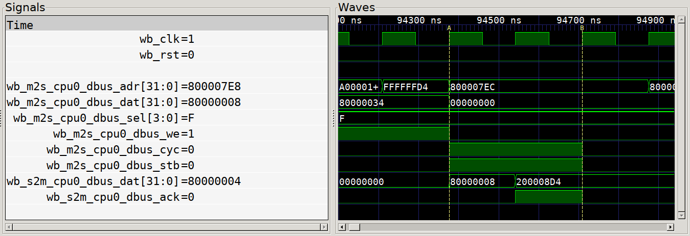
As an example, here is a trace of a wishbone transaction. At time marker A, the
master outputs the valid address, data and control lines and simultaneously
asserts the cyc and stb lines. One the next positive edge of the wishbone
clock wb_clk, we see the slave respond with new data on its output and the
assertion of the ack signal. At time marker B, the master clears the cycle
and strobe signals, ending the transaction.
Classic Wishbone Transaction
There are other signals specified in the full Wishbone spec, such as errors,
retry signals and tag data, but for many simple peripherals these signals are
not implemented. For complex designs beyond the one shown here, or for further
reference on the signals or formal properties of the bus, the full
Wishbone Spec
is an excellent reference. But for now, we know enough to be dangerous, and
create some peripherals for our CPU.
The persistence of memory
To make a soft CPU useful, it needs to be fed instructions from somewhere. It’s
also fairly common to want some amount of random access memory in excess of the
built-in registers. To solve both of these problems, let’s write a quick
memory module that can be accessed over the wishbone bus to provide either
instructions or data to our CPU. Since both ROM and RAM are similar in
behaviour here, we can reuse the same design for both. The implementation of a
minimal working memory is something like the following
(full code):
// Our main data storage. Yosys will replace this with an appropriate block ram
// resource.
parameter SIZE =512; // In 32-bit words
reg [31:0] data [SIZE];
// Each data entry is 32 bits wide, so right shift the input address
// Sub-word indexing is achived through the byte select lines
localparam addr_width = $clog2(SIZE);
wire [addr_width-1:0] data_addr = i_wb_adr[addr_width+1:2];
integer i;
always @(posedge i_clk) beginif (i_reset) begin// Under reset we can't zero the memory contents, just ensure
// that the wishbone bus returns to an idle state.
o_wb_ack <=1'b0;
endelsebegin// Always ensure that our ack strobe defaults to low
o_wb_ack <=1'b0;
// If we are being addressed, and this is not the cycle following an
// ack, we need to perform a read/write
if (i_wb_cyc & i_wb_stb &~o_wb_ack) begin// We always read/write in the same cycle, so can
// unconditionally set the ack here
o_wb_ack <=1'b1;
// Always read the data at the given address to the output register
// If this was a write operation, the data will simply be ignored
o_wb_dat <= data[data_addr];
// If this is a write, we need to do something a bit special here.
// Since this memory needs to support non-32-bit operations, we
// have to respect the byte select values. Handle this by looping
// over each bit, and only writing the corresponding word if the
// select bit is set.
if (i_wb_we) beginfor (i =0; i <4; i++) beginif (i_wb_sel[i])
data[data_addr][i*8+:8] <= i_wb_dat[i*8+:8];
endendendendend
With this, we have something that can be read and written over wishbone (and we
can even add
some test cases
for it). This looks good for RAM, but for ROM we need a way to preload our
firmware into the memory. Verilog has system functions, $readmemb and
$readmemh that can load binary or hex data into a memory from a file. So,
let’s add another small feature so that we can tell our ROM memory to
initialize itself from the firmware hex we will generate later:
// If we have been given an initial file parameter, load that
parameter INITIAL_HEX ="";
initialbeginif (INITIAL_HEX !="")
$readmemh(INITIAL_HEX, data);
end
Connecting the blocks
Now that we have a CPU with a wisbone interface, and two wishbone peripherals,
we just need to connect them all together. Writing all of the muxing and
switching logic for this by hand would be extremely tedious, but
luckily there exists an excellent tool,
wb-intercon, that does the legwork for
us.
Given a YAML description of a bus (the masters, which slaves they connect
to and what address they should see those slaves at) wb-intercon can generate
all of the verilog necessary
to mux and arbitrate the various signals.
So, to start off
with, let’s create a very simple wishbone layout that has two masters (our CPU
instruction and data bus ports) and two slaves, our ROM and RAM blocks. Note
that our ibus here only connects to the ROM, so executing from memory isn’t
allowed, but could of course be changed if you wanted to! We will arbitrarily
locate the rom at 0x20000000, and give it a max size of 4KiB. We will then
locate the RAM at 0x80000000, and only give ourselves 2KiB.
If we run this through the wb-intercon generator, which in
the full project is done as
part of the CMake build,
we end up with two files - an implementation file,
which contains the modules responsible for the address decoding and signal
multiplexing, and a header file that contains all of the signal definitions for
our various bus participants. In order to connect up our modules, in our
top gateware file
we just need to include this header and then use the generated
wires to connect up our two wishbone RAM blocks, like so:
// Include the header that defines all the wishbone net names
`include"gen/wb_intercon.vh"// CPU ROM.
// We initialize this directly from the hex file with our firmware in it
wb_ram #(
.SIZE(1024), // In 32-bit words, so 4KiB
.INITIAL_HEX("ice40_soc_fw_hex")
) cpu0_rom (
.i_clk(wb_clk),
.i_reset(reset),
.i_wb_adr(wb_m2s_cpu0_rom_adr),
[...]
.o_wb_ack(wb_s2m_cpu0_rom_ack)
);
// CPU RAM
wb_ram #(
.SIZE(512) // 2KiB
) cpu0_ram (
.i_clk(wb_clk),
.i_reset(reset),
.i_wb_adr(wb_m2s_cpu0_ram_adr),
[...]
.o_wb_ack(wb_s2m_cpu0_ram_ack)
);
Once we similarly connect the iBusWishbone and dBusWishbone signals on
our CPU,
everything is in place for us to start writing some code to run on our new
system.
Baremetal RISC-V programming
Now that we have defined our hardware, we need to start defining our firmware.
Since we do not have any operating system to handle hardware initialization and
program startup for us, we must do it ourselves. This means getting hands on
with the linker, the assembler and some low level features of the RISC-V
architecture.
Defining our layout
At the end of our firmware compilation process, we need to end up with
a series of bytes
that represent the code our CPU should run and the values of any initialized
data. We can then load these bytes into the CPU, and should be up and running.
However to get here, we need to start by defining for the compiler how to
arrange that code, and at what addresses the running program can expect to
find things. In our earlier wishbone intercon YAML, we specified that the ROM
should appear at 0x20000000, and the RAM at 0x80000000.
Since we want to locate non-volatile
data in ROM and volatile data in RAM, we need to tell the linker where these two
memories exist, and what goes into each, so that it can generate correctly
addressed loads, stores and jumps.
The way to do this is in the linker script, the complete version of which is
here.
We define our memory regions (in this case we have just 2) with a MEMORY
directive, like so:
/* Define our main memory regions - we created two memory blocks, one to act as
* RAM and one to contain our program (ROM). The address here should match the
* address we gave the memories in our wishbone memory layout.
*/
MEMORY {
ram (rwx) : ORIGIN =0x80000000, LENGTH =0x00000800
rom (rx) : ORIGIN =0x20000000, LENGTH =0x00001000
}
This tells the linker that we have two regions where we can store data, and
how much data we can safely fit in each location. Both these values must match
the values used in the gatware, or there may be subtle problems later!
Now that we have defined the regions, we need to indicate what parts of our
program live in which section. We’ll start with the code itself, or the .text
section - this should contain
our initial startup code at the very beginning, followed by the rest of our
code, and any other read-only data:
.text : {
/* Ensure that our reset vector code is at the very beginning of ROM,
* where our CPU will start execution
*/*(.reset_vector*)
/* General program code */*(.text*)
/* Ensure that the next block is aligned to a 32-bit word boundary */
. = ALIGN(4);
/* Read-only data */*(.rodata*)
} >rom /* Locate this group inside the ROM memory */
Linker Relaxation
There are various other sections that must be located, all of which may be
found in the
full linkerscript,
but the other section I will flag here is one specific to the RISC-V
architecture - the .sdata (small data) and .sbss (small bss) sections.
The problem with a 32-bit ISA with 32-bit wide instructions is that it is
impossible for a single instruction to encode an offset that can address the
entire memory space - in reality, the immediate forms of memory load/store and
jump instructions can address only up to 21 bits from the current PC / other
base pointer. What this means is that operations referencing addresses over 2^21
bits away must be broken up into two operations - one to load an immediate into
a register, and another to perform the actual operation. This can be a
significant performance problem for some code, so RISC-V includes a feature
called Linker Relaxation. When the linker is assembling the final binary, it
will attempt to emit smaller jump/load instructions by addressing them relative
to a special register, the global pointer (gp) register. This register is
expected to be set to the address 0x800 bytes past the start of the small data
section, such that it can be used as a base for single-instruction addressing.
For a fuller explanation of linker relaxation, the SiFive blog has an excellent
post
here.
What makes this relevant to us is that we have some new sections in our linker
script, that we might miss if we were to assume the same layout as some other
embedded systems. In our linker, we need to be sure to actually include the
.sdata and .sbss sections (otherwise, statically initialized variables may
silently become zero-initialized!) and export the desired location of the global
pointer. For our data section, this results in a linker directive like the
following:
/* Our data segment is special in that it has both a location in rom (where
* the data to be loaded into memory is stored) and in ram (where the data
* must be copied to before main() is called).
*/
.data : {
/* Export a symbol for the start of the data section */
_data = .;
/* Insert our actual data */*(.data*)
. = ALIGN(4);
/* Insert the small data section at the end, so that it is close to the
* small bss section at the start of the next segment
*/
__global_pointer$= . +0x800;
*(.sdata*)
. = ALIGN(4);
/* And also make a note of where the section ends */
_edata = .;
/* This section is special in having a Load Memory Address (LMA) that is
* different from the Virtual Memory Address (VMA). When the program is
* executing, it will expect the data in this section to be located at the
* VMA (in this case, in RAM). But since we need this data to be
* initialized, and RAM is volatile, it must have a different location for
* the data to be loaded _from_, the LMA. In our case, the LMA is inside the
* non-volatile ROM segment.
*/
} >ram AT >rom /* VMA in ram, LMA in rom */
Initialization
Now that we have our linker configured to locate our initialization code in the
right place, and are exporting the addresses of important features such as the
global pointer
and
initial stack pointer,
we can start writing the lowest level code for our system. This startup code
will initialize our stack, so that we can safely make function calls, the
global pointer, so that linker-relaxed addressing works, and then call into our
next section of initialization code:
# Since we need to ensure that this is the very first code the CPU runs at
# startup, we place it in a special reset vector section that we link before
# anything else in the .text region
.section.reset_vector# In order to initialize the stack pointer, we need to know where in memory
# the stack begins. Our linker script will provide this symbol.
.global_stack# Our main application entrypoint label
start:# Initialize global pointer
# Need to set norelax here, otherwise the optimizer will convert this to
# mv gp, gp which wouldn't be very useful.
.optionpush.optionnorelaxlagp, __global_pointer$.optionpop# Load the address of the _stack label into the stack pointer
lasp, _stack# Once the register file is initialized and the stack pointer is set, we can
# jump to our actual program entry point
callreset_handler# If our reset handler ever returns, just keep the CPU in an infinite loop.
loop:jloop
Once the assembly code above has initialized the state of the gp and sp
registers, we are able to safely start calling methods and executing code
beyond careful assembly, so for the next few initialization steps we jump to
the reset_handler method, which we will write in C:
// In our linker script, we defined these symbols at the start of the
// region in ROM where we need to copy initialized data from, and at the start
// and end of the data section that we need to copy that data to
externunsigned _data_loadaddr, _data, _edata;
// Likewise, the locations of the preinit, init and fini arrays are generated
// by the linker, so we need to tell the compiler that they are defined
typedefvoid (*void_fun)(void);
extern void_fun __preinit_array_start, __preinit_array_end;
extern void_fun __init_array_start, __init_array_end;
extern void_fun __fini_array_start, __fini_array_end;
// In order for the reset_handler symbol to be usable by the assembly above, we
// need to protect it from the C++ name mangler.
// Likewise, we need to assert that there exists somewhere an application
// main() that we can invoke.
extern"C" {
int main(void);
voidreset_handler(void);
}
void reset_handler(void) {
// Load the initialized .data section into place
volatileunsigned*src, *dest;
for (src =&_data_loadaddr, dest =&_data; dest <&_edata; src++, dest++) {
*dest =*src;
}
// Handle C++ constructors / anything with __attribute__(constructor)
// These regions contain an array of function pointers, so we simply need to
// iterate each and invoke them
void_fun *fp;
for (fp =&__preinit_array_start; fp <&__preinit_array_end; fp++) {
(*fp)();
}
for (fp =&__init_array_start; fp <&__init_array_end; fp++) {
(*fp)();
}
// At last, we can jump to our actual application level code
main();
// Should our application code ever exit (unusual in embedded), we may as
// well run the desctructors properly
for (fp =&__fini_array_start; fp <&__fini_array_end; fp++) {
(*fp)();
}
}
Memory-mapped IO
After building our way up from the bottom, we have finally arrived at the
application level. From here, we can implement int main() and proceed to
write firmware with impunity. But we didn’t come all this way just to run code
in isolation, we want our code to be able to reach out and interact with
the peripherals we build into our FPGA. So to that end, let’s take a look at
how memory mapped IO works from the firmware side.
We saw earlier that our CPU has two buses - an instruction bus and a data bus.
When it needs to fetch instructions, the instruction bus reaches out over
Wishbone and makes a read transaction at the relevant address. Similarly,
if a load or store is executed, the data bus will generate a Wishbone
transaction against the given location. But there is nothing that states that
location has to be a memory - we are free to have those reads and writes be
routed to any wishbone peripheral we desire. So let’s create a simple RGB LED
controller that’s accessible over wishbone, and demonstrate how we can control
and query it from our C code.
The core logic of our peripheral will look very similar to the memory we
implemented a little while earlier, except that instead of a large block ram we
will create some number of small registers to hold the data the peripheral
needs to know. In this case, let’s say that our peripheral will be an 8-bit PWM
generator with red, green and blue output channels. Since our registers can be
up to 32 bits wide, we can pack the RGB component into one register and use a
second to control the prescaler for our PWM generation. In verilog, this might
look a little like this:
// PWM prescaler register
reg [31:0] pwm_prescaler;
// BGR output compare registers
reg [7:0] ocr_b;
reg [7:0] ocr_g;
reg [7:0] ocr_r;
// Wishbone register addresses
localparam
wb_r_PWM_PRESCALER =1'b0,
wb_r_BGR_DATA =1'b1,
wb_r_MAX =1'b1;
// Since the incoming wishbone address from the CPU increments by 4 bytes, we
// need to right shift it by 2 to get our actual register index
localparam reg_sel_bits = $clog2(wb_r_MAX +1);
wire [reg_sel_bits-1:0] register_index = i_wb_adr[reg_sel_bits+1:2];
always @(posedge i_clk) beginif (i_reset) begin
o_wb_ack <=0;
pwm_prescaler <=0;
endelsebegin// As in our RAM before, we can default our ack strobe low
o_wb_ack <=1'b0;
// If we are addressed by the cyc and stb lines, and are not in the ack
// out cycle, we are in a transaction
if (i_wb_cyc && i_wb_stb &&!o_wb_ack) begin// Once again we do not have any delays, so we can ack
// unconditionally
o_wb_ack <=1'b1;
// Handle register reads
// Note that our BGR data is 24 bits, so we pad it to 32
case (register_index)
wb_r_PWM_PRESCALER: o_wb_dat <= pwm_prescaler;
wb_r_BGR_DATA: o_wb_dat <= {8'd0, ocr_b, ocr_g, ocr_r};
endcase// Handle register writes if the write enable flag is set
if (i_wb_we) begincase (register_index)
wb_r_PWM_PRESCALER: pwm_prescaler <= i_wb_dat;
wb_r_BGR_DATA:begin// For RGB writes, break out the data to the individual
// output compare registers
ocr_b <= i_wb_dat[23:16];
ocr_g <= i_wb_dat[15:8];
ocr_r <= i_wb_dat[7:0];
endendcaseendendendend
The full implementation of this module can be found
here.
Once we have granted this peripheral an entry in our wb intercon YAML and
connected it up in our
top module,
we can turn back to the firmware and take a
look at what’s necessary to interact with it. If we located our LED peripheral
at wishbone address 0x40002000, then in our C++ code if we read or write the
32-bit memory at that location, what we will actually be doing is reading or
writing the prescaler register of our LED block. It’s that easy! The only two
things we need to make sure we are clear about in our code is that
This is a volatile memory address (the compiler may not assume that the last
value written to it will be the next value read from it, or that writes may be
dropped)
We did not implement selective write logic for these registers - that is to
say, if the CPU attempts to write these registers using 8 or 16 bit wide
operations, it may corrupt the high bytes of the register! To prevent this, we
must only use 32-bit wide accesses for these registers.
The register indexing we used in our Verilog localparam is based on 32-bit
words, so the register with verilog index N is actually located in CPU memory
at N * sizeof(uint32_t) past the start of the peripheral memory. We must
therefore be careful when counting our register addresses.
To make following these rules simple, it helps to define some preprocessor
macros as follow:
// Redefines an integer constant as a dereferenced pointer to a volatile 32-bit
// memory mapped IO register
#define MMIO32(ADDR) (*(volatile uint32_t *)(ADDR))

// Defines a register with 32-bit offset OFFSET
#define REG32(BASE, OFFSET) MMIO32(BASE + (OFFSET << 2))

// Now that we have our two macros above, we can quickly make some readable
// definitions for our LED driver
#define LED_BASE            0x40002000
#define LED_PWM_PRESCALER   REG32(LED_BASE, 0)
#define LED_BGR_DATA        REG32(LED_BASE, 1)
With only that, we can now read and write these registers from our code like
another variable. Let’s finally implement a main() and cycle some colours on
our LED:
#define CPU_CLK_HZ 42'000'000
uint32_t led_states[] = {
0x000080,
0x008000,
0x800000,
0x0000FF,
0x00FF00,
0xFF0000,
};
voiddelay(uint32_t cycles ) [
while (cycles--){
asmvolatile ("nop");
}
}
int main(void) {
// Initialize our PWM prescaler to generate a 1kHz carrier with 8 bit pwm
LED_PWM_PRESCALER = (CPU_CLK_HZ /256/1'000) -1;
// Iterate through each of our LED states, with a delay so that we can
// actually see what is going on
for (int i =0; i <sizeof(led_states) /sizeof(uint32_t); i++) {
LED_BGR_DATA = led_states[i];
delay(CPU_CLK_HZ /2); // Very approximately one second
}
}
Interrupts
While our above demo is very blinky, it’s not particularly elegant - our delay
loop just burns CPU cycles, and it would be hard to do cycle counting if we
were trying to achieve a number of timed tasks at the same time.
Instead it would be a lot
more useful if we could somehow keep track of the current time, and only
advance the LED state after a given number of milliseconds.
Luckily, building a timer is very much within our reach - with enough gates we
can build anything! But how do we tie the timer back into our CPU without just
busy waiting on a timer register instead of a NOP loop? One solution to this
problem is interrupts. If we build a timer module and connect it to one of the
interrupt lines on our CPU, our CPU can then jump to an interrupt handler that
either updates our LEDs directly, or simply updates a counter we can reference
from our main loop.
Let’s start with the verilog timer module. We don’t need anything too fancy,
but we do want to be able to at least configure the prescaler for the counter
on the fly, so that we can adjust the interrupt rate in our firmware. We also
need to be able to clear the interrupt signal from the timer, so it’s back to
the Wishbone peripheral structure we are getting increasingly familiar with.
The first part of a timer is simple: we need to be able to count. In this case,
we count down from our configured prescaler to zero, then reload the prescaler
and start all over again, something like this:
// Prescaler value. Reloaded onto the downcounter on update.
reg [31:0] prescaler =32'hFFFF_FFFF;;
// Downcounter. Trigger output is latched high when this hits zero.
reg [31:0] downcounter =32'hFFFF_FFFF;;
// Trigger output signal
reg timer_trigger =0;
// Downcount until the counter reaches zero, then reload the prescaler and
// start counting down again
always @(posedge i_clk) beginif (downcounter >0) begin
downcounter <= downcounter -1;
endelsebegin
downcounter <= prescaler;
timer_trigger <=1'b1;
endend
Now that we have that, we need to add enough wishbone logic to allow for
setting the prescaler, and for clearing the timer trigger when it is set. Since
interrupts on the CPU are level-triggered, if we don’t clear the interrupt
source, the CPU will end up returning from and re-entering the timer interrupt
forever!
// Wishbone register addresses
// Each register is 32 bits wide
localparam
wb_r_PRESCALER =1'b0,
wb_r_FLAGS =1'b1,
wb_r_MAX =1'b1;
// Bit indices for the flags register
localparam
wb_r_FLAGS__TRIGGER =0;
// Since the incoming wishbone address from the CPU increments by 4 bytes, we
// need to right shift it by 2 to get our actual register index
localparam reg_sel_bits = $clog2(wb_r_MAX +1);
wire [reg_sel_bits-1:0] register_index = i_wb_adr[reg_sel_bits+1:2];
always @(posedge i_clk) begin// Default the ack signal to a zero state.
// Later writes to this register will take precedence if we are actually
// performing a wishbone transaction
o_wb_ack <=1'b0;
// If the cycle and strobe inputs are high, and this is not the cycle after
// a previous transaction, we are servicing an actual wishbone request
if (i_wb_cyc && i_wb_stb &&!o_wb_ack) begin// None of our operations take more than one cycle, so we can always
// unconditionally ack the request
o_wb_ack <=1'b1;
// To handle writing the prescaler / clearing flags, we need to check
// if this is a write request
if (i_wb_we) begin// If it is, use the address bits to select the appropriate
// register to work with
case (register_index)
wb_r_PRESCALER:begin// Load the new prescaler, and also reset the downcounter
// If we don't reset the downcounter, we run the risk that
// the previously loaded value was extremely large and will
// delay 'proper' operation at the new prescaler rate
prescaler <= i_wb_dat;
downcounter <= i_wb_dat;
endwb_r_FLAGS:begin// If this is a write to the flags register, we want to
// check which flags are being cleared.
// If the trigger bit is written, we clear the trig state.
if (i_wb_dat[wb_r_FLAGS__TRIGGER])
timer_trigger <=1'b0;
endendcaseendendend
Note - in the two preceding snippets, the timer_trigger register is written
to from two different always blocks - this is not valid verilog! If you are
going to copy parts of this module, please do so from the
full source code.
Now that we have a timer implementation, the only remaining change to make in
gateware is connect up the timer trigger output wire to the timer interrupt
input on our CPU, and to connect the timer to the wishbone bus wires we
generated with our wb_intercon file.
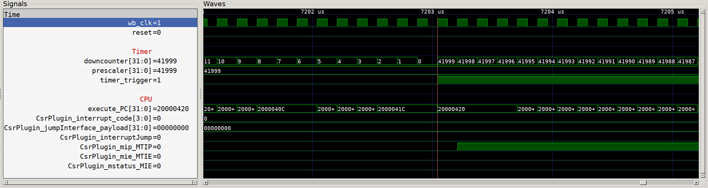
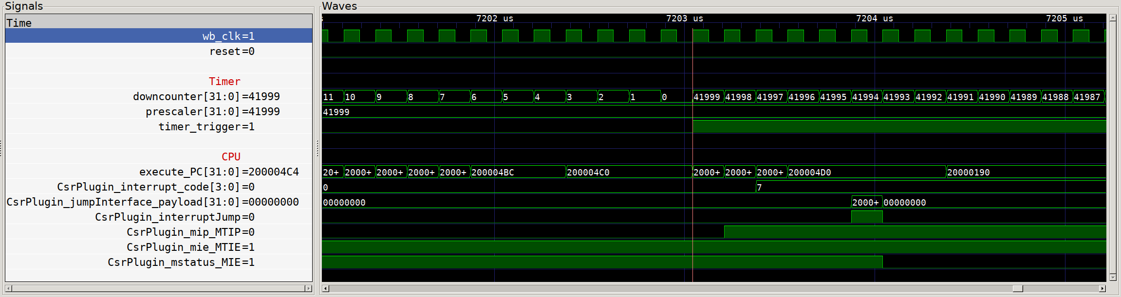
With that hooked up, our gateware is good to go! Let’s take a quick look at our
simulation and see that interrupt in action:
Timer interrupt execution?
Except… we see nothing! Our timer counts down and sets the trigger output,
but our CPU ticks along as though nothing has happened. What gives! The clue
here is the additional signals on screen - the default value of the
Configuration and Status Registers (CSRs) that relate to interrupts have all
interrupts disabled by default. So even though we see that the Machine Timer
Interrupt Pending (MTIP) flag is set, nothing happens. So we need to switch
over to our firmware and make sure that we configure the CPU properly to handle
our interrupts.
The first register we need to configure is the Machine Trap-Vector Base-Address
register, or mtvec. This register is used to store the
memory address that the CPU will jump to in the event of an interrupt.
Since the address must be 32-bit aligned, the low 2 bits are used to control
the interrupt mode, where a value of 0x0 is direct (all exceptions jump to
the mtvec address) and a value of 0x1 is vectored (interrupts set the program
counter to (mtvec + (4 * exception_code)).
In vector mode, mtvec must therefore be the start of a series of jump
statements to specific exception handlers, instead of the entry point to a
single exception handler. For simplicity we will use the non-vectored version
and work out how to handle the interrupt in software. But before we can set the
mtvec address at all, we need some sort of interrupt handler routine to point
it to, so let’s create one now.
// We need to decorate this function with __attribute__((interrupt)) so that
// the compiler knows to save/restore all register state, as well as to
// re-enable interrupts on return with the mret instruction.
void__attribute__((interrupt)) interrupt_handler(void) {
// When an interrupt occurs, the mcause register contains the interrupt type
uint32_t mcause;
asmvolatile("csrr, %0":"=r"(mcause));
// The top bit of mcause is the sync vs async exception bit, we don't
// handle that here so mask it off
mcause &=0x7FFFFFFF;
// If the cause is some number out of range of our handler table, we have
// no way to handle this interrupt! Block forever.
if (mcause >= (sizeof(vector_table) /sizeof(isr_vector))) {
while (true) {}
}
// Otherwise, we can jump to the handler listed in our vector table.
// Since we took care to order our struct to match the interrupt IDs, we can
// reinterpret it as an array for easy indexing based on mcause
((isr_vector *)&vector_table)[mcause]();
}
Now you’ll note that in the code above we made some reference to a vector
table - since we are decoding the interrupt cause ourselves, we need some
structure that contains pointers to the handlers for each of our interrupts.
To keep things well named, we use a struct that has the same layout as the
interrupt numbering scheme used by RISC-V, like so:
// Create a type alias for our exception handlers, which are void functions
typedefvoid (*isr_vector)(void);
// The basic interrupts for RISC-V are the software, timer and external
// interrupts, each of which is specified for the user, supervisor and machine
// privilege levels.
struct {
// Software interrupt
isr_vector software_user_isr =&blocking_handler,
isr_vector software_supervisor_isr =&blocking_handler,
isr_vector software__reserved =&blocking_handler,
isr_vector software_machine_isr =&blocking_handler,
// Timer interrupt
isr_vector timer_user_isr =&blocking_handler,
isr_vector timer_supervisor_isr =&blocking_handler,
isr_vector timer__reserved =&blocking_handler,
isr_vector timer_machine_isr =&timer_interrupt,
// External interrupt
isr_vector external_user_isr =&blocking_handler,
isr_vector external_supervisor_isr =&blocking_handler,
isr_vector external__reserved =&blocking_handler,
isr_vector external_machine_isr =&blocking_handler,
} vector_table;
This struct, when compiled, turns into an array of function pointers that we
can index directly with mcause. For interrupts that we don’t explicitly
handle yet, we point to a simple blocking handler that loops forever, hanging
the CPU so that we can detect something has gone wrong.
The one interrupt that we do actually want to handle properly right now, the
timer interrupt, is pointer to a timer_interrupt function, which we will
define like so:
// Our counter is modified from an interrupt context and read from a
// non-iterrupt context, so we need to mark it volatile to ensure accesses hit
// main memory each time
volatile uint32_t time_ms =0;
voidtimer_interrupt(void) {
// Increment the millisecond counter
time_ms++;
// We need to also clear the source of the interrupt, otherwise when we
// return from interrupt it will just fire again right away.
TIMER_FLAGS |= TIMER_FLAGS__PENDING;
}
Alright, we now have all the handler code that we should need once our
interrupt actually fires. However, we still have yet to actually enable
interrupts or tell the CPU where exactly to go when an interrupt is triggered.
In order to do this, let’s add some code early in our firmware initialization
that sets the relevant CSRs:
// Firstly, let's update the machine interrupt vector CSR with the address of
// our base interrupt handler.
// Since our address is 32-bit aligned, we are in non-vectored mode by default
asmvolatile("csrw mtvec, %0"::"r"(&interrupt_handler));
// We now want to enable the machine timer interrupt. To do this, we need to
// set bit 7 in the Machine Interrupt Enable (mie) register
// We use the assembler shorthand CSR Set bit instruction here for convenience
// Note that the literal 1<<7 is here marked as a register operand - the CSRS
// instruction only supports 5-bit immediates
asmvolatile("csrs mie, %0"::"r"(1<<7));
// We then need to enable machine interrupts globally, by setting bit 3 in the
// Machine Status Register (mstatus).
// Here, 1<<3 fits in the immediate form of the instruction ("i")
asmvolatile("csrs mie, %0"::"i"(1<<3));
Finally, we should have completed all the necessary legwork to get timer
interrupts running on our CPU. To verify, let’s take another look at our
simulated system:
Timer interrupt execution with MTIE and MIE enabled
Much better! We can see that the MTIE and MIE bits are now set, and that we
have a clear cycle by cycle progression of our timer output signal going high,
being registered in the CPU as a pending timer interrupt (MTIP), the
corresponding interrupt code (7) being loaded in mcause, and finally the
CSR-triggered jump to our interrupt handler at 0x200000190. If we were to
zoom out on the scope above, we would later see the timer trigger be cleared by
the write in our timer interrupt handler to the timer flags register, the
deassertion of MTIP and the return to normal code execution.
If we build and deploy this with a couple of tweaks to our colour generation
(see full code here)
we should end up with a lovely changing colour cycle running on our
dev board:
Interrupt-powered RGB cycling
The full source code for all gateware, firmware, tests and simulations used in
this post can be found
on Github here.
The repo also contains some code and peripherals that we did not cover here,
such as a buffered UART peripheral.
Design files and assembly instructions for the FPGA board shown in the image
above can be found in this previous post.
Sat, Apr 4, 2020Companion code for this post available on Github
One of the more eyecatching demonstrations of FPGAs recently has been the trend
to show off smoothly animating
LED Cubes
of various
sizes and shapes. But what goes
into making these? How do we interface with the LED panels that construct them?
And can we use those panels to show an animated GIF? In this post, I will
attempt to cover the building blocks necessary to load custom animations onto a
FPGA board
powered by the Lattice HX4K, and display those animations on a 64x64 LED panel.
All source code for the following can be found
on Github.
How do RGB panels work?
While the specific layout of the various LED panels available online
may differ, the general architecture is by and large the same.
Three sets of shift registers (one each for the red, green and blue pixel
data) have each bit of their output connected across one column of the LED grid.
This means that whatever bit pattern is shifted into these registers controls
which columns of the display will light up. However, we generally don’t want to
the same data on every line - in order to select a single row for the given
column data, the common pin of each LED in a row is connected to an output of
an address demultiplexer, which uses the address select inputs to enable only
a single row at a time. A simplified diagram of a 64-column by 32-row display
is shown below (many rows/cols have been omitted):
Subsection of common RGB panel
One thing to note about this architecture is that while it is simple in terms
of component cost, we can only actually display one unique row of data at a time.
In order to show an entire image, we need to quickly scan through displaying rows
at some speed above which the strobing is invisible to the naked eye, and the
persistence of vision effect makes the image appear solid. This sort of high speed
data shifting application is a perfect place for FPGAs, so in the rest of this
post we will try and cover getting from displaying a solid colour to full
animated GIFs with 5 bit colour channels.
If you want to follow along, I would strongly suggest building one of the
ICE40 HX4K Breakout Boards
I wrote about here,
which the code samples in this post have been written for, or a comparable
board such as
1bitsquared’s iCEBreaker.
You will also need a LED panel - the one I will be using here is
a 64x64 model with a HUB75E connector.
You can find similar panels cheaply on AliExpress (search HUB75E, 64x64), or
purchase find them at
various
other
sellers
on the internet. This panel is internally organized as two 64x32 panels, so
instead of having just the one set of RGB shift registers it instead has two,
one for the top half and one for the bottom. This doesn’t mean too much for our
design, we will just have two sets of outputs.
Finally, you will need some way to connect your FPGA board to the display. You
can either use jumper wires or a PMOD style breakout, such as
this one.
Getting started
The first thing to do with any project is get to the point where you can see
everything working (or not working) end to end. So let’s start by creating a
panel driver module that will cycle through displaying each of the 8 primary
colours (the possible permutations of R, G, B) in turn to make sure that we are
able to shift data in and advance the row selector. The first step in this is
to configure which pins on our FPGA board connect to what signals of our LED
panel. For me, I have the
PMOD to HUB75E board
connected to PMOD ports C1 and C2 on the
HX4k Breakout board, as shown:
PMOD to HUB75E adapter
This means that I can use the PMOD[] definitions from the
Placement Constraint File
for the board when interfacing with the RGB panel. So in my top level verilog
file, I can declare my inputs like so:
With our IO named in the top module, let’s create a second module to hold all
of the logic needed to drive out display, called panel_driver. To start, we
will just try and display solid colours, one after the other. Here is the full
verilog description of that module:
`default_nettype none`define CLOCK_HZ 12_000_000
module single_colour_test(
// Input clock to our panel driver
inputwire i_clk,
// Shift register controls for the column data
outputreg o_data_clock,
outputreg o_data_latch,
outputreg o_data_blank,
// Data lines to be shifted
outputreg [1:0] o_data_r,
outputreg [1:0] o_data_g,
outputreg [1:0] o_data_b,
// Inputs to the row select demux
outputreg [4:0] o_row_select
);
// How many pixels to shift per row
localparam pixels_per_row =64;
// State machine IDs
localparam
s_data_shift =0,
s_blank_set =1,
s_latch_set =2,
s_increment_row =3,
s_latch_clear =4,
s_blank_clear =5;
// Simple colour cycling logic. We will have a prescaler that counts down
// to zero twice per second, based on the frequency of our module input
// clock (`CLOCK_HZ`).
// Whenever this countdown hits zero, we will increment our colour state
// register, each bit of which is mapped to the reg, green or blue data
// channel of the RGB panel shift registers.
localparam COLOUR_CYCLE_PRESCALER = (`CLOCK_HZ/2) -1;
reg [$clog2(COLOUR_CYCLE_PRESCALER):0] colour_cycle_counter =0;
reg [2:0] colour_register;
always @(posedge i_clk) beginif (colour_cycle_counter ==0) begin
colour_register <= colour_register +1;
colour_cycle_counter <= COLOUR_CYCLE_PRESCALER;
endelse
colour_cycle_counter <= colour_cycle_counter -1;
end// Connect the output colour data lines to our colour counter
assign o_data_r = {colour_register[0], colour_register[0]};
assign o_data_g = {colour_register[1], colour_register[1]};
assign o_data_b = {colour_register[2], colour_register[2]};
// Register to keep track of where we are in our panel update state machine
reg [2:0] state = s_data_shift;
// How many pixels remain to be shifted in the 'data_shift' state
reg [7:0] pixels_to_shift =64;
always @(posedge i_clk) begincase (state)
s_data_shift:begin// Shift out new column data for this row
if (pixels_to_shift >0) begin// We have data to shift still
if (o_data_clock ==0) begin// For this test, we have hardcoded our colour output, so
// there is nothing to do per-pixel here
o_data_clock <=1;
endelsebegin
o_data_clock <=0;
pixels_to_shift <= pixels_to_shift -1;
endendelse
state <= s_blank_set;
end// In order to update the column data, these shift registers actually
// seem to require the output is disabled before they will latch new
// data. So to perform an update, we have a series of steps here that
// - Blank the output
// - Latch the new data
// - Increment to the new row address
// - Reset the latch state
// - Unblank the display.
// Each step has been made it's own state for clarity; if one wanted
// to save a little more on logic some of these steps can be merged.
s_blank_set:begin o_data_blank <=1; state <= s_latch_set; ends_latch_set:begin o_data_latch <=1; state <= s_increment_row; ends_increment_row:begin o_row_select <= o_row_select +1;
state <= s_latch_clear; ends_latch_clear:begin o_data_latch <=0; state <= s_blank_clear; ends_blank_clear:begin
o_data_blank <=0;
pixels_to_shift <= pixels_per_row;
state <= s_data_shift;
endendcaseendendmodule
If we build and deploy this to our FPGA test board, we should see the connected
LED panel flash through the 8 possible colours we have with each color channel
being fully on / off:
Full-colour test pattern
Displaying Images
So far so good - we are now able to control the colours output to the panel,
and can do so fast enough that the panel appears to be solid. However, so far
we are just displaying solid colours - not very useful. Instead, let’s add the
ability for our gateware to display one of the most popular image formats: the
animated GIF.
Our test image: nyancat
But this begs the question, how do we get all that data loaded into our FPGA?
And once it’s in there, how do we display it? If we were to store each frame of
the above GIF as a 64x64 array of bytes, we would need 64 * 63 * 3 * 11 frames
of data - that’s 132 KiB. Looking at the datasheet for our HX4K, we see that it
only has 80K ram bits - only 10K ram bytes! We will clearly need to be
more creative. If instead of using a full byte per colour pixel we shave each
channel down to 5, we can store one pixel in two bytes, using 5 bits each for
Red/Green/Blue -> 15 bits per pixel. This brings us down to 88KiB for the
entire animation, still far too large. However, it does bring us down to 8KiB
per frame - which does fit in our 10KiB of system memory. But that still
only fits one frame - in order to display an animation, we will have to have
some persistent storage that we can read each frame from into our memory buffer
so that we can blast it to the screen. Luckily, on this board, we have such a
persistent storage - the flash chip used for storing the FPGA bitstream.
The HX4K bitstream is, at maximum, 136,448 bytes (according to Lattice note
TN1248)
. However, the flash chip on the HX4K breakout we are using here is 128 megabits,
or 16 megabytes. This means that even with the bitstream using the lower part
of the flash, we can store image data in the higher address regions so that our
application can read out frame data when it needs it. So let’s write a quick
program that, given a series of input images that are 64x64 pixels, converts
each one to a packed RGB565 and then writes all of the frames, in order, to a
binary file that we can then load onto the flash of the FPGA board. The full
source of this utility, img_pack, is included in the
Github repo
that accompanies this post. In order to use it on our test image, we first need
to do a little preprocessing using ImageMagick.
# Resize the gif to 64x64 pixels, ignoring aspect ratio
convert -resize 64x64\! nyan_fullres.gif nyan_64.gif
# Convert the resized gif into individual frames
# This will generate nyan_frame-0.png through nyan_frame-11.png
convert -coalesce nyan_64.gif nyan_frame.png
# Now that we have our individual frames as images, we can use the img_pack
# tool to generate a binary representation of the gif to be loaded to our board
img_pack nyancat.bin nyan_frame-{0..11}.png
After that, if you are using the HX4K dev board you can use the
faff
tool to load the program into flash at a safe offset that won’t interfere with
the FPGA bitstream itself.
If you are using the iCEBreaker board, the iceprog has a similar option for
loading data at a specific offset.
# To load the data into flash, we can use the faff utility to interact with the
# HX4K dev board, and write the data at offset 0x800000, safely out of the way
# of the bitstream
faff --lma 0x800000 -f nyancat.bin --no-verify
# Alternately, on an iCEBreaker, the following should work:
iceprog -o 0x800000 -X nyancat.bin
Reading from Flash
Now that the data is safely on the flash, we need to be able to actually access
it from our FPGA, and then store it in our RAM buffer so that our panel driver
can then read it and blit it to our display.
The flash chip on the HX4K board, as well as those on almost all other flash
chips, share a common set of command words. All of them can be found in the
datasheet (see
here),
but the important ones here are:
0x66, 0x99: Reset enable / reset. This command series will put the device
back into a sane state to receive commands, important to do at boot since we
can’t gauarantee what operation the flash was in the middle of whenever our
gateware came online.
0xAB: Release from power down. The HX4K, after loading the bitstream, is
careful to put the flash chip into a power down state, since as far as it’s
concerned it’s done with the flash until it next needs to load the
bitstream. In order to read our frame data from it, we need to send this
instruction to first wake it up.
0x0B: Fast read. To get our pixel data out, we send this command followed by
the 24 bit start address for our read, and then after one byte worth of
delay the flash chip will output it’s data, one byte at a time, until we
stop reading. When we need to read the next frame, we just send another fast
read command and a new address, and we are good to go.
With these commands, we can think of our flash loader state machine as being:
Idle state. Wait here until we get a signal to load the next frame from
flash.
Reset state. Select the flash chip, clock out the reset command.
Wakeup state. Select the flash chip, and release it from power down.
Initiate read state. Select the flash chip, and clock out the fast read
command followed by the address data and the idle byte.
Perform read. For as many bytes as are in a frame, shift in data and store
it in our ram buffer. When we are done, return to the idle state.
A shortened version of the flash loader verilog is shown below.
The full code listing can be found
here.
// Flash commands for use later
`define FLASH_OP_RESET 16'H6699
`define FLASH_OP_FAST_READ 8'H0B
`define FLASH_OP_WAKEUP 8'HAB
always @(posedge i_clk) begincase (state)
// Default idle state. This state will only transition if the 'initiate
// read' module input is set, at which point it will latch the base
// address and start the read operation
s_idle:beginif (i_read_stb) begin
flash_read_addr <= i_read_addr;
state <= s_initiate_reset;
endend// Perform a flash chip reset. Takes advantage of our
// flush_command_buffer state, by just specifying the data to shift,
// and which state to transition to after the command operation is
// complete.
s_initiate_reset:begin// Our command buffer just needs the two reset bytes, the rest
// of the bits are don't care (zero)
command_buffer <= {`FLASH_OP_RESET, 24'b0};
cmd_buffer_bits_to_shift <=16;
flash_cs <=0;
// Once the command is done, we want to move to the wakeup step
next_state <= s_initiate_wakeup;
// Directly transition to the generalized 'flush buffer' state.
state <= s_flush_command_buffer;
end// Similar to the above, but takes the flash chip out of sleep mode
s_initiate_wakeup:begin
command_buffer <= {`FLASH_OP_WAKEUP, 32'b0};
// [...]
state <= s_flush_command_buffer;
end// Once again, we set up the data for flush_command_buffer, this time
// with the 'fast read' command and the start address we latched when
// we started the read process
s_initiate_read:begin
command_buffer <= {`FLASH_OP_FAST_READ, flash_read_addr, 8'b0};
// [...]
state <= s_flush_command_buffer;
end// State for performing a command action. Shifts out a given number of
// bits from the command buffer (MSB first), and when done transitions
// to the state idenfitied by the next_state register.
s_flush_command_buffer:beginif (cmd_buffer_bits_to_shift >0) beginif (flash_sck ==0) begin// Latch new data and perform rising edge
{flash_mosi, command_buffer} <= {command_buffer, 1'b0};
flash_sck <=1;
endelsebegin// Perform falling edge and decrement bit count
flash_sck <=0;
cmd_buffer_bits_to_shift <= cmd_buffer_bits_to_shift -1;
endendelsebegin// Done - move to continuation state
state <= next_state;
// If we aren't moving to the read state, deassert CS
if (next_state != s_shift_data)
flash_cs <=1;
endend// Here is where we actually handle the incoming data from the flash
// chip. Each 16 bit word is one pixel, so every time we successfully
// read 16 bits we write it out to a block memory using the
// ram_address, ram_data and ram_write_enable signals.
s_shift_data:begin// We are going to care about 16 bit chunks, since that's
// the interface we're using for our block RAMs
if (words_to_read ==0) begin
ram_write_enable <=0;
flash_cs <=1;
state <= s_idle;
endelsebeginif (input_bits_to_shift ==0) begin// Done shifting a word, move it to the output data
// lines and strobe the write signal
ram_data <= input_shift_data;
ram_write_enable <=1;
words_to_read <= words_to_read -1;
input_bits_to_shift <=16;
endelsebegin// If we just did a write, bring the strobe back down
// and increment the write address for next time
if (ram_write_enable) begin
ram_write_enable <=0;
ram_address <= ram_address +1;
endif (o_flash_sck ==0) begin// Set up rising edge of SPI clock
flash_mosi <=1'b0;
flash_sck <=1;
endelsebegin// Falling edge
flash_sck <=0;
input_shift_data <= {input_shift_data[14:0], i_flash_miso};
input_bits_to_shift <= input_bits_to_shift -1;
endendendendendcaseend
Simulating our Flash reader
Since reading from a flash chip is
slightly more involved than shifting out our pixel data, and a little harder to
visually debug, let’s write a quick test interface in Verilator so that we can
observe that our flash interface sends the right data with the right timings to
initialize a flash read, and that it then takes the incoming data and stores it
in the right place. Full source code for the testbench can be found
here.
To make our I/O more realistic, in our testbench we can create a fake SPI chip
that responds to read requests by keeping track of the output signals from the
flash_loader verilog module. An annotated excerpt of the flash simulator is
shown below:
// Data to to 'read'
const uint8_t *data =reinterpret_cast<const uint8_t *>("This is a test string");
constunsigned data_len = strlen(data);
// Fake flash update method, should be called after each master clock cycle of
// the simulation
void DummyFlash::eval() {
// Did the CS state change?
if (*spi_cs != last_cs) {
fprintf(stderr, "CS state: was %u, now %u\n", last_cs, *spi_cs);
// If the cs line went low on this clock cycle, then the flash chip is now
// selected. Use this as a trigger to reset our fake flash state.
if (*spi_cs ==0) {
shift_byte_index =0;
shift_bit_index =0;
*spi_miso =1;
last_sck =*spi_sck;
} else {
// Deselected. Move the miso line to a known state.
*spi_miso =1;
}
// Keep track of changes to the chip select pin.
last_cs =*spi_cs;
}
// If we aren't selected, just return
if (last_cs ==1) {
return;
}
// Did the clock transition?
if (*spi_sck != last_sck) {
last_sck =*spi_sck;
if (last_sck) {
// Posedge, increment the number of bits we have received from the
// SPI master
preamble_bit_count++;
} else {
// Negedge
// Don't shift data if this is the read preamble
if (preamble_bit_count >=40) {
// Set miso to be the next bit
*spi_miso =
data[shift_byte_index % data_len] &
(0b1000'0000>> shift_bit_index) ?1:0;
// Increment the bit index
shift_bit_index++;
// If we hit the end of the byte, increment the byte index
if (shift_bit_index >7) {
shift_bit_index =0;
shift_byte_index++;
fprintf(stderr, "New byte: %02x\n", data[shift_byte_index]);
}
}
}
}
}
In this simple flash example, we don’t actually verify the input address /
reset state of the flash, but hopefully this example gives an idea of how the
test code might be extended to perform this checking. If we then compile and
run the full testbench with tracing enabled, like so:
# Build the CMake project that contains the Verilator testbenches
mkdir tb/build
cd tb/build
cmake ../
make -j$(nproc)# Run the flash loader testbench. This will generate the flash_loader.vcd file,
# which can be examined in GTKwave
./tb_flash_loader
We get an output file that can be
loaded into GTKWave, where we can observe the communication between our flash
loader verilog, our emulated flash and the output signals to our pixel buffer
memory. By looking carefully at these signals, we can be confident that our
design will work once deployed on our actual FPGA board.
Trace of simulated flash loader reading from 'Flash'
Rendering from memory
With a module for reading our pixel data from flash, the only things remaining
to get animated images running on our LED panel is an animating counter for
triggering the load of the next frame, and then a modification to the panel
driver code to use the loaded frame data.
// Animation counter for triggering frame loads from the flash chip
localparam ANIMATION_UPDATE_PRESCALER = (`clk_hz/10) -1; // 10fps
localparam ANIMATION_FRAME_COUNT =11; // Number of frames in the animation
reg [$clog2(ANIMATION_UPDATE_PRESCALER):0] prescaler_reg =0;
always @(posedge i_clk) beginif (prescaler_reg ==0) begin// Reload the prescaler downcounter register
prescaler_reg <= ANIMATION_UPDATE_PRESCALER[$clog2(ANIMATION_UPDATE_PRESCALER):0];
// Strobe the flash load signal
flash_load_strobe <=1;
// If we have reached the final frame in the animation, go back to
// frame 0. Otherwise, just advance to the next frame.
if (frame_index == ANIMATION_FRAME_COUNT)
frame_index <=0;
else
frame_index <= frame_index +1;
endelsebegin// Downcount prescaler
prescaler_reg <= prescaler_reg -1;
flash_load_strobe <=0;
endend
[...]
// To connect our frame counter up to the flash reader, and knowing that each
// frame is 64*64*2 = 8192 bytes, we can create a wire that counts up the start
// address of each animation frame from a specified base address.
localparam FLASH_BASE =24'h80_00_00;
wire [23:0] flash_load_addr = {FLASH_BASE[23:21], frame_index, 13'b0};
For our panel driver, we can change our data output from our solid colour
registers we used earlier to the most significant red, green and blue bit of
the pixel byte. This will be enough for us to view on the panel whether we have
succeeded in loading the frame data from flash.
// On the negative edge of the serial clock cycle, set the output
// red/green/blue data. For this intermediate step, we will just set the pixel
// value to the most significant bit of that channel.
if (data_clock ==0) begin// We need to load the n'th most significant bit of each colour channel,
// based on which pixel bit index we are currently displaying
// pixel_bit_index is in range 0..4
data_r <= {i_ram_b2_data[11+ pixel_bit_index],
i_ram_b1_data[11+ pixel_bit_index]};
data_g <= {i_ram_b2_data[6+ pixel_bit_index],
i_ram_b1_data[6+ pixel_bit_index]};
data_b <= {i_ram_b2_data[0+ pixel_bit_index],
i_ram_b1_data[0+ pixel_bit_index]};
data_clock <=1;
ram_addr <= ram_addr +1;
end
With this updated gateware, if we rebuild and reflash our FPGA board we should
be greeted by something vaguely recognizable as our desired GIF output:
MSB-Only Animation running off the FPGA
Achieving colour depth
While we have managed to get an animation running on our LED panel, it’s clear
that it’s not perfect yet - we are still only using our initial 8 colours,
since each pixel is only displaying one bit of red green or blue colour. To
improve our colour representation, and make the most of all that extra pixel
information we packed into the flash, we need to get a bit smarter with our
multiplexing. We want to make sure that all 5 of our data bits are used, but we
also need to make sure that our multiplexing scheme reflects the relative
importance of each bit. Since the colour is a binary number, each bit
represents a value twice that of the less significant bit, so we should show
the most significant bit of colour information for twice as long as the next
most significant, and bit 1 should be shown for twice as long as bit 2, and so
on and so on. This means that instead of scanning the entire display once per
frame, we are actually going to scan it 5 times - the first time, we will
display the most significant bit of data for 100% of the time it takes us to
display the next row. Then, we will scan through with the next most significant
bit, at a 50% duty cycle. The bit after that at 25%, and so on.
To achieve this, we need to add just a little more code to our panel_driver
module:
// Our serial data output step takes 128 clock cycles (2 * the number of pixels
// in a row). So, if we enable the display of the row data for as long as it
// takes us to shift the new row of data, that's 100% duty cycle. If instead we
// cut off the display after 64 cycles, that's 50% duty, and so on.
// Here we'll create a short lookup table for how many cycles the display
// should be enabled, based on which bit of the colour information is being shown.
reg [8:0] time_periods_for_bit[5];
initialbegin
time_periods_for_bit[4] =128;
time_periods_for_bit[3] =64;
time_periods_for_bit[2] =32;
time_periods_for_bit[1] =16;
time_periods_for_bit[0] =8;
end// Countdown register for displaying our row data. When this hits zero, we shut
// off the output enable for the column drivers.
reg [8:0] time_periods_remaining;
// Which bit of the pixel data are we currently displaying? Counts down from
// the most significant bit (4)
reg [2:0] pixel_bit_index =4;
// [...]
// In our data shift state, we now have one extra check to perform - decrement
// the exposure time periods, and if we hit zero, disable the output
s_data_shift:begin// Expose the previous row while we do our data loading.
// Our most significant bit display time is such that it
// matches the number of cycles it takes to load data, and then
// each successive bit halves that value.
if (time_periods_remaining ==0) begin// Turn the blanking back on
data_blank <=1;
endelsebegin
time_periods_remaining <= time_periods_remaining -1;
end// [...]
// We also have a little logic to add to our blank_clear state -
s_blank_clear:begin// Load the number of time periods that we should expose this
// row for
time_periods_remaining <= time_periods_for_bit[pixel_bit_index];
// If the current row address is zero, we have done one
// full scan through the display, and should move to the
// next most significant bit of colour data
if (row_address ==0) beginif (pixel_bit_index ==0)
// If we hit the lsb, wrap to the msb
pixel_bit_index <=4;
else
pixel_bit_index <= pixel_bit_index -1;
end
And with that, we should be able to render a nice, smooth animation to our LED
panel.
Nyancat in glorious 5-bit colour
As always, full source code to replicate the results of this post is available
on Github.
If you want more details on the FPGA board used in this post, you can read
about it
here
or take a look at the design files directly
here.
If you want a refresher on what exactly an FPGA is and does,
this post may be useful.
If you want to take things to the next level with a soft RISC-V CPU and build
your own SoC,
click here.
Sun, Mar 29, 2020Companion code for this post available on Github
After going over the basic idea of what an FPGA is and running some simulations
in the last post,
the next logical step is to take things from the computer and into the real
world. To that end, this post will attempt to cover the entire journey from PCB
design to running gateware on an assembled board in such a way as to make it
accessible to those new to FPGA development. Some implementation details have
had to be left out for brevity, but every piece of CAD, firmware, and
gateware referenced in this post can be found in
this git repo
for those that want to read deeper.
The Hardware
The hardware designed to accompany this post is a breakout board consisting of
a
Lattice ICE40 series
HX4K
FPGA, one of the few FPGAs that comes in an easy(er)
to solder quad flat leaded package. The FPGA IO are broken out to 10 standard
PMOD
connectors, for a total of 80 external IO lines. There is also an ARM based
STM32F070CBT6
microcontroller, with two hardware SPIs connected across to the FPGA (one
shared with the flash), one hardware UART connected to the FPGA and a USB
interface for communicating with a host computer.
Full hardware design files can be found in the
hardware/
folder. Feel free to use this design as a
reference for further work, but if you do, bear in mind a couple of design
points.
The first is that
(most) FPGAs are volatile - they do not maintain their configuration if they are
power cycled, and so every time they turn on they must be reconfigured before
they will operate. This can be done automatically by the FPGA acting as a SPI
master to read from a flash device, by having the FPGA acting as a SPI slave
and receiving the bitstream data from a microcontroller or other device, or
over JTAG.
To make turning on our FPGA board as simple
as possible, we will include a flash chip connected to the FPGA to provide
storage for the bitstream. However, we also need some way to program the
bitstream onto the flash chip. One approach is to place an FTDI device such
as the
FT2232
on the board, which allows reading/writing the flash using
MPSSE
instructions. However, these chips are a bit expensive (Over $6 in quantity 1),
and the functions they are performing aren’t overly complex. This is why for
this design we instead use a
cheap ARM based microcontroller with USB support to perform flash
operations. In addition, the microcontroller code can be extended with
application code to extend the functionality of the system.
The second thing to take note of is that FPGAs generally have a number
of different voltage rails that must be supplied. The FPGA
core generally runs at a fairly low voltage - here 1.2V. However, FPGAs have
separate supply pins for the IO voltage level (VCCIO), which can be
set differently per IO bank if you need to interface with multiple devices at
different voltage levels. In our case, we’re going to use 3.3V as our IO
voltage, since it is fairly widely compatible and is also the voltage for our
microcontroller.
Third, one of the biggest advantages of routing FPGA designs is the lack of
constraints around pinout - since
any IO pin can be any function, we are fairly free to shuffle our connections
between FPGA and PMOD to achieve more direct routing.
However, there are some small exceptions - certain pins on the device will be
listed as being directly connected to ‘global buffers’, or other special
purpose routing constructs that provide high signal fanout / low timing skew
within the device itself. If you have any
signals coming into the FPGA that are likely to be used in many places (e.g. a
clock), it is generally advantageous to connect those signals to a hardware pin
that has a dedicated connection to one of the high-fanout internal buffers.
Finished design. 2 Layers.
Building Your Owm
If you want to build your own copy of this breakout board, you will first need
to acquire some blank PCBs.
If you have done this before, you can clone the repo
containing all of the design files (gerbers are in
hardware/gerber/)
and ship the Gerbers to your preferred PCB
manufacturer.
Alternately, or for convenience, you can
order this design directly
from PCBWay, a budget PCB house with respectable quality and turnaround time.
While you wait for your boards, you may also need to order components.
The KiCad design files are fully specified with the manufacturer and
DigiKey part numbers for all components involved. Also included in the
hardware/
folder is a DigiKey BOM
(digikey_bom.csv),
which can be
uploaded to the
DigiKey BOM Tool
and used to immediately add the necessary components to an order.
Note that the BOM item quantity is for precisely one unit - I would recommend
going through and adding whatever fudge factor you feel is reasonable to
cheaper passives and other parts you want some margin for error with.
At time of writing, the total cost of the BOM for no more than one board is
$37.60. If you intend to make more than one, the unit price will go somewhat
as you hit the price breaks.
Overview of BOM in KiCad Table Editor
Once you have the parts and boards, there are a couple other prerequisites for
assembly -
Soldering iron (TS-100 or TS-80 would be fine for this)
Flux (Massively simplifies the soldering of the QFP packages)
Fine tweezers (I recommend Rhino SW-11 or comparable)
[Optional] Board holder. I find PCBite setup to be
extremely worth it.
[Optional] Hot air rework station. The ‘858D’ hot air station is available
from many resellers at reasonably prices, and is more than adequate.
One of the design goals for this board was for it to be feasible to assemble by
hand, using only a soldering iron. To that end, all of the critical
components are leaded packages, and there are no passives smaller than 0805.
For some components (USB type-C connector J4, 12MHz oscillator X1 and RGB LEDs
D1 and U4), a hot air gun may be advantageous, but it is possible to get away
without one.
Component placement for assembly
If like me you use a fair amount of flux during assembly, I would recommend
washing the PCB afterwards using first some
flux cleaner
and an
ESD toothbrush,
followed by a rinse in some 99% isopropyl alcohol. You can then leave the board
to air dry, or apply (gentle!) heat with the hot air gun to evaporate any
remaining isopropyl.
Finished Assembly (Front)
Finished Assembly (Back)
Interfacing to the Computer
Now that we have our board assembled, we need to be able to write bitstreams
to it, otherwise it isn’t very useful. In order to do this, we’re going to need
to write some firmware for the onboard microcontroller that will allow us to
perform a programming flow along the lines of
Put the FPGA into reset
Erase and reprogram the flash
Take the FPGA out of reset
Act as an intermediary if we implement a UART on the FPGA
For that we are going to use a STM32F0 series part and the
open source
libopencm3
HAL. For more information on getting started with that programming environment,
I would recommend reading through
this series of posts.
The core of our firmware is going to be listening for incoming packets over
one USB endpoint, figuring out what operation is intended, and then potentially
responding back to the computer. The full implementation can be seen in
usb_protocol.cpp,
but that basic idea is that we use the first byte of any incoming USB packet to
determine the command. Since we have a bounded number of commands, we have a
lookup table that maps the command code to an appropriate handler function. For
example, here is the handler for the UsbProto::Opcode::FPGA_RESET_ASSERT
command, which puts the FPGA into reset in anticipation of programming:
void UsbProto::handle_fpga_reset_assert(const uint8_t *buf, int len) {
  // In order to program the flash, we want to make sure that we aren't in
  // contention with the FPGA for control over the SPI lines. The first thing
  // to do here is therefore to pull the NRESET line of the FPGA low
  FPGA::assert_reset();
  // Once the FPGA is no longer driving any signals, we can enable the hardware
  // SPI on our microcontroller, taking control of the bus.
  SPI::init();
  // Once the spi is ready, we send a few initialization commands to the flash
  // chip to ensure it is ready to perform reads / writes.
  Flash::init();
  Flash::reset();
  Flash::wakeup();
}
The vast majority of this code should apply to other boards designed around a
microcontroller programming interface in this way, so in an attempt to make
this firmware easy to port to your own projects, all pin configuration data is
contained in a single header file,
include/config.hpp,
so that it can be adapted for slightly different implementations.
To get the firmware uploaded, you will need some sort of SWD adapter
(my go-to being the
BlackMagic Debug Probe), and a
TagConnect 2050
cable in order to connect to the programming pads.
To build:
# Install ARM toolchain
sudo apt install gcc-arm-none-eabi gdb-arm-none-eabi binutils-arm-none-eabi
# Clone & build the firmware repo
git clone git@github.com:rschlaikjer/hx4k-pmod.git
cd hx4k-pmod
git submodule init
git submodule update
# Build
mkdir programmer_firmware/build
cd programmer_firmware/build
cmake ../
make -j$(nproc)
Once the binary is built, if you are using the black magic probe (and it is
connected as /dev/ttyACM0), you can flash the device by first connecting it
to power through either the USB header or auxiliary power jack, and then
building using the CMake target
fpga_programmer_flash. You should see output similar to the following:
ross@mjolnir:/h/r/P/G/f/p/build$ make fpga_programmer_flash
[ 44%] Built target libopencm3
[100%] Built target fpga_programmer_elf
Black Magic Probe (Firmware v1.6.1-311-gfbf1963) (Hardware Version 3)

Available Targets:
No. Att Driver
 1      STM32F07 M0
event_loop () at /home/ross/Programming/Github/fpga-swe-1/programmer_firmware/src/main.cpp:87
Loading section .text, size 0x29e4 lma 0x8000000
Loading section .init_array, size 0x8 lma 0x80029e4
Loading section .data, size 0x14 lma 0x80029ec
Start address 0x8001e84, load size 10752
Transfer rate: 18 KB/sec, 768 bytes/write.
Section .text, range 0x8000000 -- 0x80029e4: matched.
Section .init_array, range 0x80029e4 -- 0x80029ec: matched.
Section .data, range 0x80029ec -- 0x8002a00: matched.
Kill the program being debugged? (y or n) [answered Y; input not from terminal]
[100%] Built target fpga_programmer_flash
You should then see the board show up as a USB device, with the default VID:PID set to a generic test PID:
ross@mjolnir:/h/r/P/G/f/p/build$ lsusb -d 1209:0001
Bus 001 Device 106: ID 1209:0001 Generic pid.codes Test PID
However, this firmware is only one half of the programming flow - we also need
a program to run on the host computer and send the necessary control/data
packets to the device. To that end, I have created a tool to
Find and Flash FPGAs called
faff, which speaks the simple USB
protocol we’ve defined in the firmware. The implementation of the host side of
the USB commands can be seen in
src/usb_protocol.cpp,
and follows the same naming as used in the firmware, Requests are by and large
fairly straightforward - for example, here is the implementation for writing
data to flash:
void Session::cmd_flash_write(uint32_t addr, const uint8_t *data,
uint8_t size) {
// Our packet structure must contain
// - One byte operation (FLASH_WRITE)
// - Four byte write offset (MSB first)
// - One byte indicating how many data bytes follow
// - N data bytes to be written to flash
uint8_t cmd_out[size +6] = {
static_cast<uint8_t>(Opcode::FLASH_WRITE),
((uint8_t)(addr >>24)),
((uint8_t)(addr >>16)),
((uint8_t)(addr >>8)),
((uint8_t)(addr >>0)),
size,
};
// Copy the data to be sent into our output packet buffer
memcpy(&cmd_out[6], data, size);
// Ask libusb to send this packet to the device.
int transferred =0;
int ret =
libusb_bulk_transfer(_usb_handle, _args._usb_endpoint_tx, cmd_out,
sizeof(cmd_out), &transferred, libusb_timeout_ms);
// If libusb failed to write out this packet, we will abort here.
assert_libusb_ok(ret, "Failed to initiate flash write");
}
To build this tool, make sure you have libusb’s development headers installed,
and then build it using CMake:
# Install dependencies
sudo apt install -y build-essential cmake libusb-dev
# Clone the repo
git clone git@github.com:rschlaikjer/faff.git
# Build as a normal CMake project
mkdir faff/build
cd faff/build
cmake ../
make -j$(nproc)# Optionally
sudo cp faff /usr/local/bin
Once faff is installed and in your $PATH, we can use it to list connected
targets using the -e|--enumerate option, and then load a file using -f:
ross@mjolnir:/h/r/P/G/f/build$ ./faff -e
Searching for devices with VID:PID 1209:0001
[0] Serial: 004700254753511120303234
Found 1 devices

ross@mjolnir:/h/r/P/G/f/build$ ./faff --usb-serial 004700254753511120303234 -f top.bin
Claimed device 1209:0001 with serial 004700254753511120303234
Flash chip mfgr: 0xef, Device ID: 0x17 Unique ID: 0xe4682c404b163333
Programming block 0x00020fa0 / 0x00020fbc
Reading block 0x00020fa0 / 0x00020fbc
faff has a couple more options, which can be found by running it with the
--help flag. But for now, being able to detect and write files to the flash
is all we need.
Synthesizing Gateware
Finally, we have gotten to the point where we can actually start on the FPGA
part of this FPGA breakout board. If you haven’t already, download and install
the open source FPGA toolchain consisting of
yosys,
icestorm
(since this is an ice40 part) and
nextpnr.
Instructions for all of them are on their respective homepages.
The first thing we need to do when bringing up an FPGA board is define the pin
mapping. For this, we need a ‘Physical Constraint File’ (pcf). This is
something you generally only need to do once per hardware design, and will
then be applicable for any applications running on that hardware. The syntax is
fairly straightforward (full file for this board can be found
here),
and assigns a name to a given FPGA pin (by number, for QFx packages, or by
ball, for BGA packages):
# Input 12MHz oscillator is connected to physical pin number 21
set_io -nowarn CLK_12MHZ 21

# RGB led has three connections, on FPGA pin numbers 83-85
# Also, note that these LEDs are active LOW!
set_io -nowarn LED_R        84
set_io -nowarn LED_G        85
set_io -nowarn LED_B        83
When we then create our top-level Verilog module, we are able to use any signal
defined in the PCF file as a module connection, like so:
`default_nettype none`define CLK_HZ 12_000_000
module top(
// Input clock
inputwire CLK_12MHZ,
// RGB LEDs
outputwire LED_R,
outputwire LED_G,
outputwire LED_B
);
// To blink the LEDs at a human scale, let's have a counter that
// rolls over at approximately 4Hz. Note that this is not a proper
// prescaler - we're just getting a power of two in the right ballpark
localparam PRESCALER_4HZ = (`CLK_HZ/4) -1;
reg [$clog2(PRESCALER_4HZ):0] counter;
// And assign the LED outputs to be the higher (slower) bits of
// that counter
assign LED_R = counter[$clog2(PRESCALER_4HZ)];
assign LED_G = counter[$clog2(PRESCALER_4HZ)-1];
assign LED_B = counter[$clog2(PRESCALER_4HZ)-2];
// At every rising clock edge, increment that counter by one
always @(posedge CLK_12MHZ) begin
counter <= counter +1;
endmodule
If you cd to the
gateware/
directory in the repo that accompanies this project and run make, you
should see it synthesize, place and pack a demo bitstream that will blink some
LEDs as a sign of life. If all goes well, you should see this output:
If all goes well, you should be greeted by a green light on the MCU status
LED, and a multicoloured blink pattern from the FPGA:
Demo gateware blinking
The demo verilog provided also instructs the FPGA to echo back any UART signals
it receives. To verify that this is working properly, connect to the serial
port of the board (here ttyACM2) and try typing some characters. You should
see them show up in the serial console as they are received, echoed by the FPGA
and sent back over USB. You can connect using screen as a serial monitor
with the command screen /dev/ttyACM2 2000000, where 2000000 is the baudrate.
Hopefully some of the information or tooling here is useful for those looking
to get their feet wet programming or designing FPGA based boards. If you end up
using faff or the associated firmware and there is a feature you think would
be generally useful, feel free to mention it on either the
faff repo
or the
hardware/firmware repo
issues tab.
For a larger project based on this breakout board, take a look at either
this post
that works through creating an animated GIF display panel using an RGB LED
matrix, or
this post
for creating your own SoC with a RISC-V CPU.
Fri, Dec 13, 2019Companion code for this post available on Github
In this (increasingly lengthy) post, I will attempt to cover enough of a
grounding in what an FPGA is and how it is configured that others out there can
start to play around with writing HDL of their own. Be warned that I am by no
means an expert on FPGAs, and so information here is only correct to the best
of my own knowledge!
There is no required hardware to follow along with this post. All tools are open source. I will
assume some familiarity with C build tools.
What is an FPGA?
An FPGA (Field Programmable Gate Array)
is, first and foremost, NOT A CPU (out of the box, at least). Rather than being
a fixed silicon implementation that can only execute what it was made for (like
a 74 series logic chip, or an Intel CPU, or an ARM based microcontroller), an
FPGA is a large array of basic building blocks, each of which generally
implements a very simple
truth table. However, on their own
these individual blocks would be fairly useless. In order to combine
them to form more complex logic, FPGAs also contain a dense set of programmable
connections between these logic elements, generally referred to as the routing
fabric. If you envision each logic element as a single chip, the routing fabric
is a set of programmable wires between all of them.
FPGAs can have between hundreds and hundreds of thousands of these
individual logic elements, and it is through the combination of many of these
blocks that complex logic like conventional CPUs and dedicated special-purpose
computation engines can be constructed.
Let’s take a look at a current FPGA, the
Lattice ECP5.
The figure below is
taken from the Lattice
ECP5 family datasheet,
and shows the Programmable Functional Unit, one of the lower level
blocks that make up the FPGA fabric.
ECP5 Programmable Functional Unit (PFU) block
We can see here the two main building blocks within an FPGA - the LUT
(Look Up Table) and the Flip Flop (FF).
In this case, we have a LUT4 - a lookup
table with 4 inputs. With one LUT4, you have 2⁴ = 16 possible states that you
can encode. This means that you can trivially perform calculations like AND,
OR, XOR, NOT (with up to 4 1-bit inputs) with a single LUT by loading in the
appropriate
truth table. You are of course not limited to those common boolean operations - a LUT
can implement any truth table you may want to create. If it helps to think
about FPGAs as compared to discrete logic ICs, an FPGA is essentially hundreds
of thousands of individual 74xx logic chips, waiting to be connected together.
Thus, anything you could create by hand with discrete logic can also be
represented inside the FPGA, without having to breadboard and jumper wire each
individual logic element by hand.
The other core primitive here is the
Flip-Flop,
usually of the D variety. These are necessary for buffering outputs of
combinatorial logic (LUTs), or as storage for small data (e.g. registers) that
you may use in your design.
In addition to the LUT and FF basic elements, many FPGAs also contain some
amount of random access memory (RAM), usually of 2-3 distinct classes:
Block RAM: Large contiguous blocks of dedicated SRAM. There are a fixed
number of these available in a given FPGA, with individual sizes usually
ranging from 8KiB to 32KiB. They generally support various access widths.
Distributed RAM: Generally smaller (on the order of several byte) blocks of
RAM, distributed throughout the FPGA fabric. May be faster access than the
block ram.
LUT RAM: This term refers to using ordinary LUT+FF blocks as memory storage,
wherein the FF stores one bit of data and the LUT contains the logic
necessary for handling stores to that bit. Since this uses ordinary LUTs,
the amount of LUT RAM available to you is bounded more by your tradeoff
between logic requirements and data storage requirements.
Finally, FPGAs may implement some other special purpose logic elements that can
be tied into your design. These include Multiply/Accumulate (MAC) elements,
Digital Signal Processing (DSP) elements or full peripherals such as SPIs.
These blocks can vary significantly between different FPGA families, so refer
to the relevant datasheet for more details on these.
Why would you use an FPGA?
Given the wide and varied offerings of increasingly cheap microcontrollers on
the market, you may wonder why you might want to use an FPGA in a project.
There are after all negatives to FPGAs - they come with next to
nothing built-in. If you get a new microcontroller, you already
have a CPU core, peripherals (GPIO, I2C, SPI, etc.) and an interconnect bus
tying it all together. With a few bytes of assembly instructions you can write
some peripheral registers, and you’re good to go.
With an FPGA, at first power on you have absolutely nothing. If you want a CPU,
you have to buy, download or build the HDL for one from scratch. You need to implement
any connections between your CPU and the peripherals (which, again, YOU have to
build into the design).
However, the power of the FPGA is in the fact that you
can do these things. If you have a microcontroller, and realize you need
another I2C master, you need to go out and buy a different chip.
If you discover that your SPI communication is experiencing clock skew, you
have to feed the reflected clock back into another SPI peripheral to account
for it, which might not be possible or might again require changing out your
hardware.
But with an FPGA, if you need a new I2C master, you just generate one.
If you need to tweak the details of how your SPI
master works, you just change the HDL that describes it. Add more FIFO space,
clock the MISO line from a reflected CLK signal, whatever you want to change is
within your power to change, provided you have the LUTs to do so.
This makes FPGAs very powerful for applications where you need to do something
specific and do it fast, such as
Number crunching very wide numbers (you can build a vectorized ALU with as
many bits as you have gates for)
Performing multiple computations steps in a guaranteed real-time
Parallel computation (If you want 16 Z80 processors, just add them)
Hardware Description Languages
What they are not
Now that we have somewhat of a handle on what an FPGA is and when we might want
to use one, let’s take a look at how we actually “program” an FPGA. The first
thing that I would say to anyone coming to FPGAs from a software background is
that:
FPGA Hardware Description Languages are NOT programming languages
This is a very important thing to un-learn, otherwise you may struggle to
intuitively understand what is happening in HDLs such as Verilog or VHDL. A programming
language like C essentially defines a set of steps that are serial by default.
For example, in this code:
int a =3;
int b = a +2;
return a + b;
As a programmer, you understand that we first assign 3 to a. Only after we have
finished assigning 3 to a do we calculate b, and only after that do we add it
back to a and return.
This makes sense, since the interface CPUs present to
the end user is that they run one instruction, then the next, and so on (even
if under the hood, they are speculatively executing and reordering your
instructions).
However, on an FPGA, all operations can be thought of as
parallel by default. Let’s take a look at the following Verilog:
In this module, the calculations for o_ret1 and o_ret2 happen continuously.
This is to say that whenever the input values change, the output also updates,
as fast as it is physically possible for the FPGA to do so.
Since each statement will instantiate
it’s own hardware, these two calculations will also run parallel to each other,
such that o_ret1 and o_ret2 will both update at the same time (plus or minus
variance in the propagation delay of their logic paths), rather than one after
the other.
In general, any statement in verilog that stands on its own
will be encoded as it’s own logic, and so happen in parallel with other
statements. Since what’s happening is not that your code is taking turns to
execute on a shared hardware resource (CPU), your code is defining the hardware
resources that calculate the desired results. And this points at the crux of the difference:
Programming Languages define a series of steps.
Hardware Description
Languages define how to build a circuit.
Not internalizing this difference early on led me personally to spend a lot of
time struggling to understand HDLs. Don’t make my mistake!
What they are
As stated before, Hardware Description Languages (HDLs) define circuits. In
Verilog, the two basic elements are reg and wire:
reg is used to define a 1 or more bit data register (a D flip-flop).
Registers are required anywhere you need to store data, either for computation
on later clock cycles or as an output buffer from a module so that downstream
logic can sample the data without seeing intermediate states of the next
computation.
wire is used to connect things together (like a real wire in the discrete
chips analogy). Wires cannot store state - you must use a register
for that. Wires however can encode combinatorial logic - it is
valid to assign a wire to the result of a simple calculation, such as
the sum of two other signals. Synthesis tools may insert registers wire
definitions if it would be required for the design to work.
Groups of registers and wires can be encapsulated into Modules, which can
then be used as their own primitives. This allows us to quickly build up
complex behaviours from progressively smaller primitives. A single clocked
flip-flop can be repeated to create a FIFO, which can be included as part of a
peripheral, several of which can be connected to the same bus for a CPU to
access.
What assignment means
In Verilog, there exist three assignment operators:
=: Blocking assignment. Verilog may not execute any following statements
in the same always block until this assignment has been evaluated.
The left hand side of the assignment
will have the new value when the next statement is executed. Use for
combinatorial logic.
<=: Non-blocking assignment. These statements are executed in two steps by
the verilog abstract machine: On the first timestep, all right-hand side values
are computed, effectively in parallel. On the second timestep, all left-hand
values are updated with the calculated right-hand values. Use for sequential
logic.
assign: Continuous assignment. Equivalent to = when used outside of an
always block.
Blocking assignment is primarily useful for combinatorial / unclocked logic. It
allows you to write logic that looks more like a classical program - for
example, the following defines a simple combinatorial logic setup:
module blocking(inputwire a, inputwire b, inputwire c, outputwire d);
wire a_xor_b = a ^ b;
assign d = c & a_xor_b;
endmodule
Non-blocking assignments are what make sequential logic possible, because of the
two-step evaluation. The two time quanta represent
the time just before and the time just after the trigger event for the block
containing the logic (a positive clock edge, for example). If we consider the
following simple divide by 2 oscillator design we can see why this is important:
If we were to use a blocking assignment here, assigning o_clk to itself
would be unresolvable!
However, with the two time-steps of the non-blocking assignment this allows
triggered logic to function properly - on the first time quanta the new value
(the inversion of o_clk) is calculated, and then only on the second is
it updated. It is then stable until the next update event.
Combinatorial Logic
Using just our knowledge of wires and assignments,
let’s see if we can create a module that
will add two (one-bit) numbers together, in addition to a carry-in and carry-out
bit. This is known as a
Full Adder.
//// A full-adder circuit with combinatorial logic
// We start by defining our new module, with the name 'full_adder'
module full_adder(
// We have three inputs to our module, the two bits to be added
// as well as the carry-in value.
// By default, a wire is one bit wide.
inputwire in_a,
inputwire in_b,
inputwire in_carry,
// We will output two things: the sum result, as well as whether
// the sum overflowed (the carry-out).
outputwire out_sum,
outputwire out_carry
);
// The truth table for a fill adder is like so:
// A B Cin | Sum Cout
// --------|--------
// 0 0 0 | 0 0
// 1 0 0 | 1 0
// 0 1 0 | 1 0
// 1 1 0 | 0 1
// 0 0 1 | 1 0
// 1 0 1 | 0 1
// 0 1 1 | 0 1
// 1 1 1 | 1 1
// Based on the truth table, we can represent the sum as the XOR
// of all three input signals.
assign out_sum = in_a ^ in_b ^ in_carry;
// The carry bit is set if either
// - Both A and B are set
// - The Carry in is set and either A or B is set
assign out_carry = (in_a & in_b) | (in_carry & (in_a ^ in_b));
endmodule
To see what exactly this verilog will synthesize to, we can use
Yosys
to read the verilog and generate a flowchart showing each generated primitive
and the connections between them. The yosys invocation I use for this is like
so:
yosys -q << EOF
read_verilog full_adder.v; // Read in our verilog file
hierarchy -check; // Check and expand the design hierarchy
proc; opt; // Convert all processes in the design with logic, then optimize
fsm; opt;  // Extract and optimize the finite state machines in the design
show full_adder; // Generate and display a graphviz output of the full_adder module
EOF
This command on the module above should result in an output that looks a bit
like this:
Synthesized Full Adder
The inputs/outputs of our module can be seen in the octagonal labels. From
there we can follow the connections to the lower-level blocks that yosys has
used to implement our design. If we follow the out_sum label backwards, we
can see that the in_carry value is XORed with the output of the XOR of the
in_a and in_b signals, which satisfies the wire assignment we made above in
the module definition. Similarly, we can see the logic blocks that make up the
calculation of out_carry. Notably, we have no buffers in this design - all of
these wire assignments are continuous assignments. out_carry and out_sum
will update as fast as possible when any of in_a, in_b or in_carry
change, bounded only by the propagation delay of the FPGA you might run this
on.
Sequential Logic
As with discrete electronics, one doesn’t always want a purely asynchronous
setup. Adding a clock and buffers to a design allow for real hold times for
data buses, and avoids potential instabilities during long calculation chains.
The same is true on FPGAs - while combinatorial logic is good for small chunks
of logic, it is generally the case that you will want to tie it into a
sequential design for usage. As an example, let’s take the full adder we wrote
above and make a 4-bit synchronous adder with it.
// Clocked adder of 4-bit numbers, with overflow signal
module adder_4b(
// Input clock. At the positive edge of this clock, we will update the
// value of our output data register.
inputwire i_clk,
// Input 4-bit words to add. Syntax for multi-bit signals is
// [num_bits-1:0] (so a 4 bit signal is [3:0]). Individual bits or
// groups of bits an be accessed using similar notation - signal[1] is
// the 1st it of that signal. signal[2:1] would be a two-bit slice
// of signal.
inputwire [3:0] in_a,
inputwire [3:0] in_b,
// Output data buffer containing the result of the addition.
// Note that this is a reg, not a wire.
outputreg [3:0] out_sum,
// Single output bit indicating if the addition overflowed
outputreg out_overflow
);
// Define two internal wires. We need these to connect the full adder
// elements together as a bus that we can then load into our output buffer.
wire [3:0] full_adder_sum;
wire [3:0] full_adder_carry_outs;
// We now need 4 full adders, with the carry out of each one fed into
// the carry in of the next.
// We could write out all of these by hand, but there exists a verilog
// keyword 'generate', which makes repeated declaration of elements like
// this a lot simpler.
// Because our first adder is special, we need to keep it outside the loop
full_adder adder_0(
// Take the 0'th bit of the input words as operands
in_a[0], in_b[0],
// Since this is the first bit, the carry-in can be hard-coded as 0.
1'b0,
// The output signals can be connected into the bus we made above so
// that they can be used by the next adder
full_adder_sum[0],
full_adder_carry_outs[0]
);
// Now we can generate the rest of the adders.
// First, we need to define a loop variable for the generate, like
// we would in any programming language
genvar i;
// Counting from 1 to the total number of bits in the operands, generate
// a new full adder that operates on that bit of the input words, plus
// the carry of the prevoius adder.
generate// We use the function $bits to get the width of our in_a parameter, so
// that if it changes we don't need to modify this code.
for (i =1; i <$bits(in_a); i++)
full_adder adder(
// Add the i'th bit of both operands
in_a[i],
in_b[i],
// Use the carry-in from the previous adder
full_adder_carry_outs[i-1],
// Connect our sum output to the full adder bus
full_adder_sum[i],
// Likewise connect our carry out so that it can be used by
// the next full adder
full_adder_carry_outs[i]
);
endgenerate// Now we can set up the sequential logic part of this adder.
// For clock or other event-driven signals, we need a sensitivity
// selector. Whenever the conditions in parenthesis are met, the
// body of the block will execute.
always @(posedge i_clk) begin// At the positive clock edge, we want to take the current value
// that is being calculated using combinatorial logic by the full
// adder, and copy that data into our output data buffer.
// For this, we use the non-blocking assignment operator, <=
out_sum <= full_adder_sum;
// Similarly, we take the final carry bit of the adder and use
// that as our overflow indicator.
out_overflow <= full_adder_carry_outs[$bits(in_a)-1];
endendmodule
Now that we have defined our 4 bit adder, let’s open it in a flowchart the same
was as we did for our single bit full adder. Note that you may need to include
the full_adder module definition (or a dummy implementation) in the same file
as your 4-bit adder for yosys to synthesize.
Clocked 4-Bit Adder
There is a lot more going on here! On the far left we can see our initial full
adder, with the zero’th bits of the input operands and a literal 0 bit as
inputs. The outputs then go off to the wire buses we defined, and we can see
the block of generated adder modules in the center. At the end, the final carry
bit goes to a D flip flop, which is clocked by our i_clk signal. Similarly,
the output sum data is fed to a 4-bit DFF that is also clocked.
Simulating with Verilator
In order to test and debug our HDL code, we could deploy it directly to a
physical FPGA and hope for the best, but it can be much easier to first
simulate parts or all of the design on the computer, allowing us to control
and observe signals at a very low level, and to trace execution of the HDL over
an arbitrary number of clock cycles. For Verilog, there exists an open source
tool called
Verilator
that can take your Verilog source code and convert it to ordinary C code, which
can then be linked against test benches of your own design. Let’s verify that
our 4-bit adder works properly by creating a test bench that tests every
possible combination of 4-bit values, and asserts that the result is correct.
First, we’re going to create a CMake based verilator setup (supported only on
more recent versions of verilator, I recommend at least 4.023). In our
CMakeLists.txt, let’s add the following:
cmake_minimum_required(VERSION3.8)project(four_bit_adder)# We need to locate the verilator install path.
# If this doesn't work off the bat on your system, try setting
# the VERILATOR_ROOT environment variable to your install location.
# On a default install, this will be /usr/local/share/verilator
find_package(verilatorHINTS$ENV{VERILATOR_ROOT}${VERILATOR_ROOT})if (NOTverilator_FOUND)message(FATAL_ERROR"Could not find Verilator. Install or set $VERILATOR_ROOT")endif()# Create our testbench executable.
# We will have just the one testbench source file.
add_executable(adder_testbenchadder_testbench.cpp)# Based on how I understand the verilator plugin to work, if you specify several
# verilog sources in the same target it will pick a top level module and
# only export the interface for that module. If you want to be able to poke
# around in lower-level modules, it seems that you need to specify them
# individually. To make this easier, I put all the sources in a list here
# so that I can add targets for them iteratively.
set(VERILOG_SOURCES${PROJECT_SOURCE_DIR}/full_adder.v${PROJECT_SOURCE_DIR}/adder_4b.v
)# For each of the verilog sources defined above, create a verilate target
foreach(SOURCE${VERILOG_SOURCES})# We need to speicify an existing executable target to add the verilog sources
# and includes to. We also speicfy here that we want to build support
# for signal tracing
verilate(adder_testbenchCOVERAGETRACEINCLUDE_DIRS"${PROJECT_SOURCE_DIR}"VERILATOR_ARGS-O2-x-assign0SOURCES${SOURCE})endforeach()
Now that we have a framework to build our testbench, let’s write something
fairly straightforward in C. We will manually toggle the clock line while
writing all our test inputs to the adder. We will then take the output and
assert it matches what we calculate with C.
#include<stdlib.h>#include<verilated.h>#include<verilated_vcd_c.h>#include<Vadder_4b.h>#include<Vfull_adder.h>intmain(int argc, char**argv) {
// Initialize Verilator
Verilated::commandArgs(argc, argv);
// Enable trace
Verilated::traceEverOn(true);
// Create our trace output
VerilatedVcdC *vcd_trace =new VerilatedVcdC();
// Create an instance of our module under test, in this case the 4-bit adder
Vadder_4b *adder =new Vadder_4b();
// Trace all of the adder signals for the duration of the run
// 99 here is the maximum trace depth
adder->trace(vcd_trace, 99);
// Output the trace file
vcd_trace->open("adder_testbench.vcd");
// We need to keep track of what the time is for the trace file.
// We will increment this every time we toggle the clock
uint64_t trace_tick =0;
// For each possible 4-bit input a
for (unsigned in_a =0; in_a < (1<<4); in_a++) {
// For each possible 4-bit input b
for (unsigned in_b =0; in_b < (1<<4); in_b++) {
// Negative edge of the clock
adder->i_clk =0;
// During the low clock period, set the input data for the adder
adder->in_a = in_a;
adder->in_b = in_b;
// Evaluate any changes triggered by the falling edge
// This includes the combinatorial logic in our design
adder->eval();
// Dump the current state of all signals to the trace file
vcd_trace->dump(trace_tick++);
// Positive edge of the clock
adder->i_clk =1;
// Evaluate any changes triggered by the falling edge
adder->eval();
// Dump the current state of all signals to the trace file
vcd_trace->dump(trace_tick++);
// The adder should now have updated to show the new data on the output
// buffer. Assert that the value and the overflow flag are correct.
constunsigned expected = in_a + in_b;
constunsigned expected_4bit = expected &0b1111;
constbool expected_carry = expected >0b1111;
// Check the sum is correct
if (adder->out_sum != expected_4bit) {
fprintf(stderr, "Bad result: %u + %u should be %u, got %u\n", in_a,
in_b, expected, adder->out_sum);
exit(EXIT_FAILURE);
}
// Check the carry is correct
if (expected_carry != adder->out_overflow) {
fprintf(stderr,
"Bad result: %u + %u should set carry flag to %u, got %u\n",
in_a, in_b, expected_carry, adder->out_overflow);
exit(EXIT_FAILURE);
}
}
}
// Flush the trace data
vcd_trace->flush();
// Close the trace
vcd_trace->close();
// Testbench complete
exit(EXIT_SUCCESS);
}
Now, if we build and run our testbench like so:
mkdir build
cd build
cmake ../
./adder_testbench
We should see… nothing! Our asserts should pass, and the testbench won’t
error out. We should also see that in the same directory from which we ran the
testbench, an adder_testbench.vcd file will have been created. This contains
the data of all the signals during our test case. We can open this file in
GTKWave or another wave viewer. If we click
on the TOP block in the SST tree, we should see the signals that are the
inputs and outputs to our four bit adder appear in the list view below.
Select all of them and hit ‘Append’ to place these signals on the scope view to
the right. Now you can scroll through time and observe that at the negative
edge of each clock, we set the new input data for the adder (this could also be
done at the posedge. At the following positive edge, we can see that the output
of the adder module correctly updates with the sum and overflow value.
Trace output for our 4-bit adder testbench
Hopefully with this foundation, you feel comfortable writing, viewing the
generated logic for and testing your own simple logic blocks.
The full source code for the snippets listed in this post can be found
on Github.
If you have any corrections or improvements to suggest, feel free to do so.
In the
next post,
we create and deploy to an FPGA breakout board based on the Lattice Ice40 HX4k.
After that, we use it to create an
Animated GIF display
on an LED panel and a
RISC-V based SoC.
Sat, Aug 17, 2019Companion code for this post available on Github
This is the sixth post in a series on the STM32 series of MCUs.
The previous post, on memory sections and ITCM, can be found
here.
When building embedded software, it can sometimes be challenging to determine
the root cause of a failure. You have no operating system to fall back on, and
if you are coming from a non-embedded background may not know about some of the
low-level behaviours that can be leveraged to make finding certain bugs a
little easier. In this post, I’ll go over in detail the steps to connect an
interactive debugger to your embedded system, as well as how you can make
interrupt problems easier to diagnose.
Connecting using GDB
If you have worked on applications software in either C or C++ for some time,
here’s a good chance you will at least have heard of GDB. As one of the more
venerable debuggers, it supports an incredible number of targets, including
(to my knowledge) the entire ARM Cortex ecosystem.
There are a plethora of ARM programming and debug adapters on the market, such
as:
For the purposes of this post, we will be using the cheap and powerful
Black Magic Probe (BMP).
This probe comes with a standard 10-pin SWD header, and a 4-pin UART connector.
Both of these have level-shifted output between 1.7 and 5V, and the probe can
also supply 3.3V power to targets if necessary. Even better, the probe runs an
implementation of the GDB server protocol, meaning that it can be connected to
GDB with no additional software dependencies, unlike some other tools.
To get started with the black magic probe, you’ll first need to connect it to
your device under test. For this you can use the included 0.127mm pitch SWD
connector, or other standard cable such as the popular TagConnect
TC-2050 cable, which
eliminates the need for costly headers.
Two example connections of the probe, one with the included SWD cable, and one
with a TagConnect cable, are shown here:
Example connections of Black Magic Probe
Once your cable is connected, and the device is powered up, it’s time to fire
up GDB. If you don’t already have it, you can install it and the rest of
the GNU ARM toolchain on Debian based
systems with the following command:
For other systems, you can install GDB by following the instructions
here.
Now that we have GDB ready, we need to load up the program we’re debugging and
connect to our probe. To do that, we first start GDB with the elf as our first
argument:
$ arm-none-eabi-gdb my_program.elf
GNU gdb (7.12-6+9+b2) 7.12.0.20161007-git
Copyright (C) 2016 Free Software Foundation, Inc.
# Connect to the black magic probe as a target. There are two serial ports
# exposed by the device - the first is the GDB server, the second is a
# passthrough to the UART pins on the device. The exact path to the serial
# devices will vary by OS.
(gdb) target extended-remote /dev/ttyACM0
# Now that we have told GDB to use the BMP as a target, we can invoke
# some extra commands. The first will be to scan for serial wire debug targets,
# which should return the MCU that we wish to connect to.
(gdb) monitor swdp scan
# Now that we've scanned and identified the device we want to connect to, we
# can start debugging it by attaching. In this case we want the first (and only)
# target. Invoking the attach command will automatically halt the device and
# show the current stack frame.
(gdb) attach 1
If you find yourself typing in these commands a lot, I’d recommend putting them
all in a file called .gdbinit in your working directory. This will cause GDB to
automatically run them on startup, saving you some time if you are repeatedly
closing and reopening GDB to connect to the same system.
Note that you may need to set the configuration value
set auto-load safe-path /
in the .gdbinit in your home directory to allow loading of arbitrary
.gdbinit scripts. To be more secure, use a more specific path than /, otherwise
malicious source trees could cause you to run arbitrary GDB commands.
Now that we are connected to the device, we can interact with it almost as
though it were a program runnig on our local machine, but with a few extra
commands. I’ll list a couple things I use frequently here, but do consult the
GDB manual
both for more details about these commands and for other useful
invocations. All commands shown below can be shortened to the character in
[].
# Print an expression. Expression can be a variable, function, macro, etc.
> [p]rint myvar / MY_DEBUG_MACRO / *((uint32_t*)0xDEADBEEF)# Exampine one or more memory addresses.
> e[x]amine my_array
> x/10ub 0xDEADBEEF # Print 10 unsigned bytes starting at 0xDEADBEEF
> x/s 0xDEADBEEF # Print the C-string starting at 0xDEADBEEF
# Breakpoints
> [b]reakpoint main # Create breakpoint on entry of method main()
> b my_code.cpp:123 # Create breakpoint at line 123 of my_code.cpp
> [d]elete 2# Delete breakpoint number 2
# Memory watchpoints
> watch my_var # Trigger breakpoint if my_var changes
# Trigger breakpoint if the integer value located at 0xDEADBEEF changes
> watch watch *(int *) 0xDEADBEEF
# Control flow
> [n]ext # Advance execution to next line of code
> [ni](next instruction)# Advance execution to next assembly instruction
> [c]ontinue # Run until breakpoint or user interrupt (ctrl-c)
> [r]un # Start program over from beginning
# Information
> info locals # Print all local variables and their values
> info registers # Print the contents of all CPU registers
> info breakpoints # Print all the currently active breakpoints
# Flashing
> file my_program.elf # Select the active binary
> load # Flash the microcontroller with the active file
> compare-sections # Verify the microcontroller code matches the active file
# Dump memory range 0x0 to 0xFFFF to file out.bin as raw binary data
> dump binary memory out.bin 0x0 0xFFFF
As an added tip, if your program is compiled using a makefile
any make commands entered inside of GDB will be run normally, allowing you to
rebuild and re-flash your microcontroller without ever leaving your GDB session.
Fault Handlers
While the GDB commands above should handle a lot of debugging needs, there will
still be some cases (generally due to interrupts) where the control flow of the
CPU is hard to follow. In cases like these, implementation of the ARM hard
fault interrupt, as well as providing default implementations for all user
interrupts, can be very useful.
If your code enables an interrupt but doesn’t implement the associated
handler, or causes a processor fault by attempting to execute an invalid
instruction or access invalid memory, the ARM core will jump to the Hard Fault
Handler, which is an interrupt common to the entire Cortex-M family.
Implementing this interrupt handler, and using it to provide error feedback,
can save many hours of second guessing your code.
Generally, your HAL library (such as
CMSIS,
or in this example series,
libopencm3)
will provide a weakly linked implementation of these system interrupt handlers.
In order to provide your own, all you need to do is implement it, which will
override the weakly linked one in the HAL.
When you do implement the hardfault handler, the first thing you will want to
do is determine which stack pointer was in use when the program crashed (this
is mainly relevant for applications making use of an RTOS or other system that
takes advantage of multiple hardware stacks).
When an exception or interrupt handler is entered, the processor updates
the link register with a special value, EXC_RETURN. The full details of this
behaviour can be found in the
ARMv7-M reference manual
section B1.5.8, but for
our purposes the salient bit is bit 2, which determines whether the return
stack is the main stack, or a process stack. By testing the link register
against the pattern (1 << 2), we can determine which stack point was in use
when the exception occurred, and pass the appropriate one through to our
generalized exception handler.
I’ve seen a couple hardfault handler implementations online that require a CPU
supporting conditional execution, which isn’t present on the Cortex-M0 series
processors. Here’s a fault handler that should be generic enough to work on all
ARMv7-M processors, at the cost of a few extra instructions:
voidhard_fault_handler(void) {
__asm(
"MRS r0, MSP\n"// Default to the Main Stack Pointer
"MOV r1, lr\n"// Load the current link register value
"MOVS r2, #4\n"// Load constant 4
"TST r1, r2\n"// Test whether we are in master or thread mode
"BEQ base_fault_handler\n"// If in master mode, MSP is correct.
"MRS r0, PSP\n"// If we weren't in master mode, load PSP instead
"B base_fault_handler"); // Jump to the fault handler.
}
With this bridge method in place, we can write the meat of our fault handler
code. We take as input the stack pointer address that was determined by our
assembly bridge, and gather some pertinent information about the crash into
local variables for inspection.
// Core ARM interrupt names. These interrupts are the same across the family.
staticconstchar*system_interrupt_names[16] = {
"SP_Main", "Reset", "NMI", "Hard Fault",
"MemManage", "BusFault", "UsageFault", "Reserved",
"Reserved", "Reserved", "Reserved", "SVCall",
"DebugMonitor", "Reserved", "PendSV", "SysTick"};
voidbase_fault_handler(uint32_t stack[]) {
// The implementation of these fault handler printf methods will depend on
// how you have set your microcontroller up for debugging - they can either
// be semihosting instructions, write data to ITM stimulus ports if you
// are using a CPU that supports TRACESWO, or maybe write to a dedicated
// debug UART
fault_handler_printf("Fault encountered!\n");
staticchar buf[64];
// Get the fault cause. Volatile to prevent compiler elision.
constvolatile uint8_t active_interrupt = arm::scb::ICSR &0xFF;
// Interrupt numbers below 16 are core system interrupts, we know their names
if (active_interrupt <16) {
sprintf_(buf, "Cause: %s (%u)\n", system_interrupt_names[active_interrupt],
active_interrupt);
} else {
// External (user) interrupt. Must be looked up in the datasheet specific
// to this processor / microcontroller.
sprintf_(buf, "Unimplemented user interrupt %u\n", active_interrupt -16);
}
fault_handler_printf(buf);
fault_handler_printf("Saved register state:\n");
dump_registers(stack);
__asmvolatile("BKPT #01");
while (1) {
}
}
If you were to have GDB
attached to your microcontroller when this handler is hit, you will
automatically hit the breakpoint triggered by __asm volatile ("BKPT 01"), and
be able to get a summary of what went wrong by asking GDB for info locals,
as well as investigate the additional information printed out over our serial
console:
GDB info locals command output
In addition to the variables in the above method, we call a dump_registers method
to interpret and print the values of the calling stack frame that were saved by
the CPU before it jumped to the exception handler.
The list of registers, and the
order in which they appear, is listed in section B1.5.6 of the ARM reference
manual. We can use this info to generate some more debug output, like so:
This works well as a generic fault handler, but there are some cases where we
may want to also include some additional information. For example, if a memory
fault occurs, there are several potential causes that we can flag up, as well
as the address at which the fault occurred. So for handling memory faults, we
could add a handler function such as the following:
voidmem_manage_handler(void) {
// Pull the MMFSR data out into variables for easy inspection
// Variables are volatile to prevent compiler elision
constvolatilebool mmfar_valid =
arm::scb::CFSR & arm::scb::CFSR_MMFSR_MMARVALID;
constvolatilebool fp_lazy_error =
arm::scb::CFSR & arm::scb::CFSR_MMFSR_MLSPERR;
constvolatilebool exception_entry_error =
arm::scb::CFSR & arm::scb::CFSR_MMFSR_MSTKERR;
constvolatilebool exception_exit_error =
arm::scb::CFSR & arm::scb::CFSR_MMFSR_MUNSTKERR;
constvolatilebool data_access_error =
arm::scb::CFSR & arm::scb::CFSR_MMFSR_DACCVIOL;
constvolatilebool instruction_access_error =
arm::scb::CFSR & arm::scb::CFSR_MMFSR_IACCVIOL;
// Pull the MMFAR address
constvolatile uint32_t mmfar_address = arm::scb::MMFAR;
// Trigger a breakpoint
__asmvolatile("BKPT #01");
}
If you have an MPU and trigger a write violation, or try and perform operations
with an invalid alignment, you will trigger this method and like before can get
the problem at a glance with info locals:
Memfault handler locals after null deference
In the output above, we can see that the MemManage Fault Address Register
(MMFAR) has been loaded with the address of the error, that the MMFAR address
is at 0x0, and that the access type was a data access. In other words, a null
pointer dereference!
If you want to have several exception vectors map to the same handler, a useful
trick is to alias those methods using an __attribute__
directive like so:
In order to keep my registers organized, I like to nest them in C++ namespaces
instead of having a huge list of preprocessor macros (as can be seen in the
methods above). In order to make defining
registers simple, and still allow the compiler to optimize nicely, I use
a template like the one below to generate references to each ARM register:
namespace arm {
// Convenience template for taking an integer register address and converting
// to a reference to that address.
template<typename T>constexpr T &Register(uint32_t addr) {
return*reinterpret_cast<T *>(addr);
}
// Typedefs for register references of 32, 16 and 8 bits.
using Reg32 =volatile uint32_t;
using Reg16 =volatile uint16_t;
using Reg8 =volatile uint8_t;
} // namespace arm
Using that template, we can then go through and quickly define each of the
registers in the ARM System Control Block (SCB).
namespace arm {
namespace scb {
// Interrupt control and state register (RW)
static Reg32 &ICSR = Register<uint32_t>(0xE000ED04);
// Configurable Fault Status Register
static Reg32 &CFSR = Register<uint32_t>(0xE000ED28);
// MemManage Fault Address Register
static Reg32 &MMFAR = Register<uint32_t>(0xE000ED34);
//// Register subfields
// CFSR
// 1 if MMFAR has valid contents
const uint32_t CFSR_MMFSR_MMARVALID = (1<<7);
// 1 if fault occurred during FP lazy state preservation
const uint32_t CFSR_MMFSR_MLSPERR = (1<<5);
// 1 if fault occurred on exception entry
const uint32_t CFSR_MMFSR_MSTKERR = (1<<4);
// 1 if fauly occurred on exception return
const uint32_t CFSR_MMFSR_MUNSTKERR = (1<<3);
// 1 if a data access violation occurred
const uint32_t CFSR_MMFSR_DACCVIOL = (1<<1);
// 1 if an eXecute Never violation has occurred
const uint32_t CFSR_MMFSR_IACCVIOL = (1<<0);
} // namespace scb
} // namespace arm
With any modern compiler, these constants will be nicely inlined, resulting in
zero runtime overhead compared to the old-school #define method. Depending on
how you like to write your code, either method will work just as well; this is
more a personal preference point than anything else.
Hopefully some of this information comes in useful when debugging your own
embedded projects. As ever, a Github repo containg some example code is
available here.
Sun, Aug 11, 2019Companion code for this post available on Github
If you just want to cut to the chase and flash your own badge with the
Chameleon firmware, grab
this build
and jump to the “Flashing the badge” section.
This year at DEFCON, we were lucky enough to be provided with another
electronic badge, this time courtesy of
Joe Grand. The badge is a very sleek design
featuring a quartz face, lanyard mounting straps and a Kinetis KL27 series
microcontroller (specifically, a
KL27P64M48SF2
).
The badge also has an unusual communication mechanism, an
NXH2261UKNear-Field Magnetic
Induction
chipset and antenna.
This year the core badge hardware was the same across badge types, the only
differences being a ‘badge type’ byte in the firmware for each badge, and
various colours of quartz on the non-human badges.
Human Badge, Front and Back
Some more information on the badge itself, including pictures of all the badge
types, can be found on
Joe Grand’s Website.
If one wanted to complete the badge without any trickery, they would need to go
around the conference interacting with all of the other badge types, including
a select few ‘magic’ badges, in order to complete their badge. If we peek the
source code of the badge, we can see exactly what’s needed:
// Bit masks for badge quest flags
#define FLAG_0_MASK 0x01 // Any Valid Communication
#define FLAG_1_MASK 0x02 // Talk/Speaker
#define FLAG_2_MASK 0x04 // Village
#define FLAG_3_MASK 0x08 // Contest & Events
#define FLAG_4_MASK 0x10 // Arts & Entertainment
#define FLAG_5_MASK 0x20 // Parties
#define FLAG_6_MASK 0x40 /* Group Chat (all 6 gemstone colors:
                          Human/Contest/Artist/CFP/Uber +
                          Goon + Speaker + Vendor + Press + Village) */
To save yourself some walking and learn a bit more about the badge
firmware, read on and we’ll cover two ways to complete the badge the hardware
hacking way.
Prerequisites
In order to debug or flash your device, you’ll need one of the many ARM
programmers available.
Joe Grand
recommended
NXP’s own
LPC-Link 2
but you can likely use any debug probe like the
Segger J-Link ($$),
or the
Black Magic Probe (much
more affordable),
which is what I’ll be using.
You will also need a particular TagConnect cable, the
TC-2050-IDC-NL-050-ALL,
or some fine gauge wire and a steady hand. If you plan on developing many of
your own ARM based designs, I would strongly recommend you pick up the cable.
The convenience and cost savings of not having to place .127” pin headers
quickly makes up for the price of the cable. You may also want to pick up some
cable retaining clips,
which make extended debugging require one fewer
arms.
If you intend to compile for or flash your badge, you will also need the GCC
ARM toolchain, which you can install using your package manager of choice:
Our initial goal was to solve the badge “legit” (for some definition of the
word), by not rewriting the firmware in any way. For this method, you will need
to populate the 1.8V serial headers on the opposite side to the tag-connect
pads. This method will require two badges, and the workflow goes like this:
On badge A, we connect our favourite debugger (GDB) over SWD
We then overwrite the game state in memory, tricking that badge into thinking
it is solved. This is not persistent across reboots (since it’s only a change
to SRAM), but will be good enough for now.
We then un-halt the CPU on badge A, and connect to it over UART.
On the UART, now that the badge is ‘complete’ we have three extra options -
one of which is ‘craft packet’. We can use this to spoof packets from other
badge types.
On badge A, we iterate through broadcasting all badge types (with magic bit
set), and after two rounds of this bade B will be complete, as though it had
actually interacted with the real badges
We can now reboot badge A, which reverts to being a normal, zero progress
badge.
In order to trick badge A into thinking it’s complete, we first need to figure
our what memory location holds the game state variable. I’m not skilled at RE,
so instead I’ll cheat a little, and use the linker map, which is available on
the
DEFCON media
server.
As a quick recap for those that haven’t seen linker maps before, the map
contains the load and virtual address of all variables and functions in the
finished binary. It can come in extremely helpful when debugging embedded
systems, as we’ll see here. If we search through the map file for the
badge_state variable, we can see that it’s located at SRAM address
0x1ffffcdc:
This means that to trick our badge, we just need to overwrite this one memory
address. To do that, we’ll connect to the badge over SWD (check the “Flashing
the badge” section below for a more thorough explanation of this process) in
order to debug it using GDB.
Once you’ve attached to the badge, there’s only one necessary command to set
the flags:
set {char}0x1ffffcdc = 7
Once you’ve done that, hit c for continue to un-halt the badge CPU. You can
now connect the four serial lines of the black magic probe to the UART pinout
on the opposite side of the battery. With the badge face down and the SWD
connector to the south, the staggered pinout for serial is GND (black),
TX (green), RX(purple), VCC (red). Unlike with some of the other programmers,
you must connect the power line of the black magic probe in order to power the
on-board level shifter. With other programmers, be aware that they may attempt
to power the badge themselves, and applying voltages over the expected 1.8V
badge voltage may cook your badge.
Now that you have your game state updated, when you connect to the serial
console using screen /dev/ttyACM1 115200, you should be greeted with three
additional options:
Extended serial commandset on complete badge
The last of these, ‘Update Transmit Packet’, is what we’ll be using to get our
B badge to complete. If we take a look at the firmware, we can see how the
packets are constructed:
struct packet_of_infamy // data packet for NFMI transfer
{
  uint32_t uid;   // unique ID
  uint8_t type;   // badge type
  uint8_t magic;  // magic token (1 = enabled)
  uint8_t flags;  // game flags (packed, MSB unused)
  uint8_t unused; // unused
};
With this info, we can craft our own packets, masquerading as any badge we want.
Here’s a complete list of badge types, and the command you need to send in
order to become them:
Human   U 772502840001ff00
Goon    U 772502840101ff00
Speaker U 772502840201ff00
Vendor  U 772502840301ff00
Press   U 772502840401ff00
Village U 772502840501ff00
Contest U 772502840601ff00
Artist  U 772502840701ff00
CFP     U 772502840800ff00
Uber    U 772502840901ff00
After manually cycling through these on badge A to unlock badge B, you can then
reset badge A and do the same for it, resulting in two ‘legitimately’ unlocked
badges. Of course, if that’s not enough for you, we can take it one step
further: automating the process by building a Chameleon badge.
Second Approach: Building a Chameleon
After spending several hours manually rotating packets to advance other badges,
we decided it was time to automate the process. Since the firmware is freely
available on the
DEFCON Media Server
we can grab it, modify it to our heart’s content and then flash it to our
badge. The first stumbling block I hit is that the software is written to rely
on NXP’s own libc implementation, Redlib, and downloading the official NXP
toolchain on the DEFCON wifi was going to take 8 hours. Instead of that, I
rewrote the software slightly to use Newlib, which is packaged along with the
GCC ARM toolchain. The full modified firmware building against newlib-nano
(and including the chameleon patches) is available in
this Github repo.
Once we have the original firmware building, we can go about editing it to
broadcast as every other badge type. In order to hook this in, there are two
main changes to be made. The first is that we need some way of keeping track of
time - the systick implementaion Joe used here only acts as a blocking countdown timer,
since he’d just been using it for delays. Since we want to keep an idea of how
long we’ve been broadcasting as one badge, we need to add a second counter we
can use as monotonic time. This is a quick two line change:
Now, every time the SysTick interrupt is generated, as well as decrementing the
delay timer we will also increment our own monotonic timer.
The SysTick timer is configured to interrupt every 1ms, however it is also
paused when the badge enters sleep mode, which it does while not actively
transmitting / receiving packets. Since our timer will only advance during
transmit, we can use a relatively short interval in our code, since it will get
stretched out as the chipset sleeps. With the timer in place, the patch for a
‘chameleon’ badge is relatively straightforward, and is added at the top of the
while (1) block in main():
// Outside our loop, declare our state variables:
static uint32_t state_change_timer =0;
// Inside our while(1) loop, handle the chameleon code
if (g_monotonicTime > state_change_timer +1000) {
// If it's been 1000 systicks since we last changed our badge state, it's
// time to update. First, reset our timer to the current monotonicTime.
state_change_timer = g_monotonicTime;
// Now, increment our badge type by 1, changing our identity.
nxhTxPacket.type = nxhTxPacket.type +1;
// If we've cycled through all the way to UBER (which is currently read only
// as Human, and so not particularly useful to broadcast) then go back to the
// beginning, skipping human and starting at Goon.
if (nxhTxPacket.type >= UBER) {
nxhTxPacket.type = GOON;
}
// Having changed our packet struct, we now need to load it into the
// NXH2261 to be broadcast.
if (KL_UpdatePacket_NXH2261(nxhTxPacket)) {
// If we fail once, try again. Joe seems to do this elsewhere in the code.
if (KL_UpdatePacket_NXH2261(nxhTxPacket)) {
// If we fail a second time, give up and log a message.
PRINTF(msg_nfmi_packet_err);
}
}
}
There are some other fun things you can do in the firmware, such as enabling a
longer version of
everyone’s favourite song,
or editing your LED pattern, but for the
purposes of this post those are left as exercise to the reader. Once you’ve
made your mods, from the Firmware/Debug folder you can run
make dc27_badge.axf to rebuild the firmware. If all goes well, you should get
a nice printout of your memory utilization and a success message:
Memory region         Used Size  Region Size  %age Used
   PROGRAM_FLASH:       58224 B        64 KB     88.84%
            SRAM:        5228 B        16 KB     31.91%
         USB_RAM:          0 GB        512 B      0.00%
Finished building target: dc27_badge.axf
Flashing the badge
Now that we have our updated badge firmware, it’s time to flash. I’ll assume
a black magic probe here, for other probes please consult their manuals.
The first thing we need to do is update the firmware on our black magic probe.
There seems to be a bug in the latest official firmware (at time of writing,
1.6.1) where the KL27x64 series is not recognized properly, and will show up as
a generic Cortex-M part. This causes the flashing to fail, since the KL27x64
require a specific flash unlock code before programming.
To update your black magic probe, clone the firmware repo from
Github
build it with make and then perform a DFU update on your probe with the
following command:
Now that the firmware is updated, we can connect to the badge. You will first
need to either
Remove the quartz face of your badge (gently) with a shim
Cut down the length of your tagconnect locating pins so that they are ~0.5mm
shorter than the pogo pins
Removing the quartz will keep your cable intact, and allow you to clip the
cable in place for longer development sessions. The adhesive is strong enough
that it can survive being carefully removed and reattached a few times.
Once you have connected the tag-connect cable to the badge one way or the
other, it is time to fire up arm-none-eabi-gdb and do our dirty work. Once
you have GDB open, we first need to point it to the black magic probe as our
remote debugging tool. To do this, we use the command
target extended-remote /dev/ttyACM0, where /dev/ttyACM0 should be the first
of the two serial endpoints exposed by the black magic probe.
Now that we have GDB connected to the probe, we can scan for devices, using
monitor swdp scan. This should return a list of two devices for the DEFCON
badge: the chipset, and a recovery mode that I have not explored.
N.B: If your scan doesn’t return KL27x64 M0+, and instead returns ‘Generic
Cortex-M’, close GDB and retry. This seems to be a race condition of some
sort.
Since we want to debug the main chip, we attach to it using attach 1, which
halts the core and prints our current stack frame. A successful attach
session should look somewhat like the following:
Successful attach over GDB
Now that we are hooked up and ready to go, flashing the badge is relatively
straightforward: we need to select the file to load using
file /path/to/dc27_badge.axf, and then to program the badge we just need to
run load. If you don’t want to compile your own firmware, you can usethis buildof a chameleon badge that I’ve created.
Once you run load, you should see output like the following:
Firmware flashing over GDB
Once the load is complete, your badge will still be in a halt state. To get it
running, either hit c for continue in GDB, or detach the probe and power
cycle the badge. You should now have your own chameleon or otherwise custom
firmware loaded up!
Wrapup
If this all seemed interesting, don’t be afraid to try it! For some more
reading on developing for embedded ARM systems you can check out
this tutorial series,
and to keep abreast of the progress hacking next year’s badge, join the
Hack the Badge
slack for discussion.
You can also check out some other writeups of the badge, by some of the great
people I met at the HHV this year:
This is the fifth post in a series on the STM32 series of MCUs.
The previous post, on CANbus, can be found
here.
As core frequencies increase, the performance penalty of loading instructions
and data from slow flash memories increase. For a modern core such as the
STM32F750 running at 216MHz, a single flash read can stall the CPU for 8
cycles. Luckily, on these faster cores exist mechanisms to ameliorate or
eliminate these stalls. Here I will go over two methods: loading functions into
SRAM for zero-wait-state execution, and enabling of the built-in I-cache on
certain Cortex-M processors.
Executing from SRAM
Above a certain core frequency, it is no longer possible for the attached flash
memory to keep up. This results in the need for ‘wait states’ inside the CPU -
in order to progress to the next instruction, the CPU must stall and wait for
the fetch from flash to complete. Even worse, the faster your CPU frequency
gets, the more pronounced this problem becomes.
A first solution to this, that works on all embedded microcontrollers which
allow executing from memory, is to simply copy the code to be executed from
flash into SRAM once at startup, and then run it from there afterwards.
Since most microcontrollers have single-cycle access latency for SRAM, this can
increase execution time significantly. Even on microcontrollers that support
some amount of prefetching, copying functions to memory can be useful for code
that must execute in deterministic time, or that is frequently jumped to from
unpredictable locations (for example, interrupt service routines).
Luckily, there is a way to achieve this with GNU utilities. By
default, all code will be placed into the .text section by your compiler.
But it doesn’t have to! We can create our own sections, and do as we please
with them. So for now, let’s create a section called sram_func and designate
a function as being part of this section. First, let’s edit our linker script
to tell it where the new section should go, and what it should contain.
/* Presumably, you already have a section like this defining the physical layout
of your particular microcontroller */
MEMORY
{
rom (rx) : ORIGIN =0x08000000, LENGTH =64K
ram (rwx) : ORIGIN =0x20000000, LENGTH =320K
}
/* Other existing directives should likely be kept above this new section,
unless you already have something fancy going on and know better *//* Now, we can create a new section definition */
SECTIONS {
.sram_func : { /* Our new section will be called .sram_func *//* This creates a new variable, accessible from our C code, which points
to the start address of our newly created section, in memory.
The reason for this will become apparent later. */
__sram_func_start = .;
/* We now tell the linker that into the .sram_func section it should place
all of the section data we will later tag as 'sram_func'. */*(sram_func)
/* Pad the end of our section if necessary to ensure that it is aligned on a
32-bit word boundary */
. = ALIGN(4);
/* We now take the end address of this new section, and make it also
available to the program. */
__sram_func_end = .;
} >ram AT>rom /* These two directives control the LMA and VMA for this section:
we state that it should be stored in rom (so that it can
actually be programmed onto your microcontroller), but
referenced at a location inside our ram segment. *//* For our final directive, we need to know the location in ROM to load
the data _from_ at the start of execution. */
__sram_func_loadaddr = LOADADDR(.sram_func);
}
Now that we have a place to put these functions, we can tell GCC to place them
there using a small __attribute__ directive:
__attribute__((section("sram_func")))
void exti1_isr(void) {
    // Body of a time-sensitive interrupt goes here
    gpio_set(GPIOA, GPIO1);
    // [...]
    gpio_clear(GPIOA, GPIO1);
}
With the addition of our __attribute__ field, gcc now knows to keep our
function in a new section, and we can verify this with objdump:
$ arm-none-eabi-nm -f sysv -C my_elf_file
Name                  Value   Class        Type         Size     Line  Section
[...]
exti0_isr           |080017fc|   W  |              FUNC|00000014|     |.text
exti1_isr           |20000330|   T  |              FUNC|00000028|     |.sram_func
exti2_isr           |080017fc|   W  |              FUNC|00000014|     |.text
[...]
As you can see, the ISR we just tagged as being destined for sram_func is
no longer in the .text section, and the location of the symbol is not in the
0x0800 0000 ROM section, but the 0x2000 0000 SRAM area. So far so good, but
if we were to deploy this code to the device now, as soon as we actually
triggered the ISR we would almost certainly encounter a segmentation fault.
This is because we’ve told the linker that this code is located in RAM, but
haven’t actually set up a method to actually move that code into RAM - when
the microcontroller resets, that memory space will be initialized to junk.
In order to fix this, we need to add some code at the very start of our
application to actually read the data for the sram_func section out of ROM
and copy it into RAM, where it can then be called. To do so, we use the three
variables we defined earlier as part of the linker script:
// The variables defined in our linker script are available to us as externed
// unsigned words, the locations of which denote our sections.
externunsigned __sram_func_start, __sram_func_end, __sram_func_loadaddr;
// Our sram_func_start and sram_func_end variables are located at the start and
// end of the memory space that we want to copy data into.
// The loadaddr variable is located in ROM, at the start of where the data to
// be copied is stored.
// Using these three variables, we can quickly copy the code across.
volatileunsigned*src =&__sram_func_loadaddr;
volatileunsigned*dest =&__sram_func_start;
while (dest <&__sram_func_end) {
*dest =*src;
src++;
dest++;
}
Now that we’ve done that, let’s verify that this is indeed faster. As a
testbed, I have a STM32F7 series MCU running at 216MHz. I have configured an
EXTI interrupt that is triggered on rising edges, and when fired sets and
clears a GPIO. The pin driving the EXTI interrupt is then connected to a
function generator running at 1Hz, and the input function and GPIO pin are
connected to a scope. Here is a representative trigger of the ISR running from
flash memory, where the blue trace is the input signal, and the purple trace
is the pin toggled by the ISR:
Interrupt latency running from flash
We can see that after the trigger pin goes high, we have a delay of almost
exactly 400ns before the ISR triggers and pulls the GPIO pin high. At 216MHz,
that’s close to 100 clock cycles! This is rather poor overhead, and for
applications that make extensive use of interrupts, the delays will add up. Now
let’s see what happens when we instead run our ISR out of SRAM:
Interrupt latency running from SRAM
Not bad! The latency between the trigger going high and the GPIO going high has
been cut in half, and the total execution time of the ISR has also dropped by a
little under 200ns itself.
ITCM RAM
While loading code into memory can be useful for performance, it comes at the
obvious tradeoff of taking up additional space. Luckily, on some ARM platforms
exists a section of memory called ITCM, or the Instruction Tightly Coupled
Memory. Unlike its sister memory, the DTCM, the ITCM block can only be
accessed by the CPU, and not at all by peripherals such as DMA controllers. It
is also not located in a contiguous memory space with the rest of the system
memories: at least on the STM32F750, it is located at address 0x0000 0000,
unlike the rest of the volatile memories located at 0x2000 0000. Since it’s
so isolated, if you have it it is an excellent location for any functions you
may want to load into RAM.
Block diagram of STM32F750 with ITCM highlighted
To use the ITCM as a space for functions that need to be able to execute
quickly, we can edit our linker script from above with two small changes:
MEMORY {
rom (rx) : ORIGIN =0x08000000, LENGTH =64K
ram (rwx) : ORIGIN =0x20000000, LENGTH =320K
/* Here we add a new memory region: the ITCM RAM */
itcm (rwx) : ORIGIN =0x00000000, LENGTH =16K
}
SECTIONS {
.sram_func : {
__sram_func_start = .;
*(sram_func)
. = ALIGN(4);
__sram_func_end = .;
} >itcm AT>rom /* Instead of ram, we load to itcm */
__sram_func_loadaddr = LOADADDR(.sram_func);
}
No changes need to be made to our code that loads the function data from ROM,
since after a recompilation the variables we used will automatically point at
the new data location. Any functions loaded into memory in this block will not
count against the memory space available to the program for heap, stack and
globals.
I-Cache
Eagle-eyed readers may also notice another memory hidden away in the block
diagram above:
Block diagram of STM32F750 with I-Cache highlighted
Regardless of whether you use the manual memory loading above (which I would
recommend for methods you need to guarantee run without wait states), you can
gain an often significant general performance enhancement simply by enabling
the L1 I-cache built directly into the ARM core (on models that have it, that
is. Consult your data sheet!)
Unlike the ITCM RAM, the cache does not require manual management other than
being turned on. To do so, we can follow the instructions from the
ARM V7-M Architecture Reference
Manual
in section B2.2, “Caches and branch predictors”. As the document states, all
caches are disabled at startup. To enable the I-cache, we need to first
invalidate it, and then set a bit in the Cache Control Register to enable it.
We only need two registers for this, so the code is relatively straightforward:
// Writing to the ICIALLU completely invalidates the entire instruction cache
#define ICIALLU (*(volatile uint32_t *)(0xE000EF50))
// The Configuration and Control Register contains the control bits for
// enabling/disabling caches
#define ARM_CCR (*(volatile uint32_t *)(0xE000ED14))
// We will also define two macros for data and instruction barriers
define __dsb asm__volatile__("dsb":::"memory")
define __isb asm __volatile__("isb":::"memory")
// Synchronize
__dsb; __isb;
// Invalidate the instruction cache
ICIALLU =0UL;
// Re-synchronize
__dsb; __isb;
// Enable the I-cache
SCB->CCR |= (1<<17);
// Force a final resync and clear of the instruction pipeline
__dsb; __isb;
You’ll note the inclusion of several dsb and isb blocks -
since we’re messing with instruction caches, it’s a good idea to add
some explicit synchronization barriers to the code. We will use DSB to prevent
execution from continuing before all in-flight memory accesses are complete.
We will also use ISB to flush the processor pipeline, forcing all following
instructions to be re-fetched.
Note that our inline assembly also specifies
the ‘memory’ clobber
flag since it
may change the global state, and so should not be reordered away by the
compiler.
When this cache is enabled, common codepaths will start to benefit passively.
Even our already-optimized ISR will gain a little more performance from
I-caching of GPIO manipulation code called from the ISR that wasn’t itself
loaded into ITCM ram:
Interrupt latency running from RAM with I-Cache enabled
With these two tricks, you can unlock a significant amount of extra performance
from your embedded system, and can even go further by enabling the D-cache also
present in higher-spec ARM cores. However, be advised that with the D-cache
comes pitfalls when it comes to non-TCM memories and DMA transfers.
Sat, Apr 6, 2019Companion code for this post available on Github
This is the fourth post in a series on the STM32 series of MCUs and
libopencm3. The previous post, on SPI and DMA, can be found
here.
What is CANBus?
The CAN bus is a multi-master, low data rate bus for communicating between
controllers in environments with potentially high EMI. Initially designed for
automotive applications, it is becoming increasingly used in general automation
environments as well as by hobbyists. Electrically, CAN uses a differential
pair of signals, CANH and CANL, to send data on the bus. In order to transmit a
logic ‘1’ (also known as ‘recessive’ in CAN parlance), the differential voltage
of the lines is left at 0.
To transmit a logic ‘0’ (dominant), the voltage between the lines is
driven high. This means that any node transmitting a 0 will override the
transmission of a node that is simultaneously trying to transmit a 1.
It is this mechanism that allows for the priority system in a CAN
network - since each CAN message begins with the message ID, starting from the
MSB, any controller asserting a logic ‘0’ on the bus will clobber a controller
attempting to transmit a logic ‘1’. Since all transmitters read the bus as they
transmit, this clobbering can be detected by the controller with the lower
priority transmission, which will back off until the bus is clear again. This
protocol is therefore categorized as ‘CSMA/CD+AMP’, or Carrier Sense Multiple
Access / Collision Detection + Arbitration on Message Priority.
CAN Signalling, courtesy of Wikipedia
Why would I use CAN?
When transferring data between two microcontroller systems, people are probably
already familiar with I2C and SPI, which are commonly used for low (I2C,
100-400kHz) or high (SPI, 100MHz+) speed data transfer between ICs. However,
both of these protocols are really intended for operation over a short
distance, ideally on the same board. Running I2C or SPI off-board, even for
relatively short distances, can start to result in bit errors at higher speeds
or in the presence of interference.
The electrical integrity problems with I2C and SPI can be alleviated by using
differential signals,
as is the case with RS422/485. This allows RS485 to transmit data at high
(multiple megabit) speeds over distances of 300-900 feet. This might satisfy
our reliability or distance requirements, but none of these protocols bake in
support for multi-master communication - SPI is very strongly based around a
single-master design, and while I2C does allow for multiple devices to control
the bus, there is no built-in arbitration support. Similarly for RS485, the
application developer must roll their own packet structure and arbitration to
handle bus contention.
CANBus performs quite well on some of these points, being:
Differential for signal integrity
Inherently multi-master
Low component count (single transceiver IC + termination)
Available in MCUs costing as little as a dollar
Checksummed for data integrity
However, CANbus does have some drawbacks that make it a poor fit for other
applications. These include:
Very limited packet size of 8 bytes
Maximum bus frequency much lower then SPI or RS485
Maximum bus size of ~64 nodes
Termination may need to be adjusted as nodes are added/removed
When deciding whether or not to use CAN, be sure to think carefully about the
requirements of your application and whether or not CAN is the best fit.
Electrical specifications
For ‘High speed’ CAN (~512 Kbps), all
controllers (nodes) in the system must be connected to a linear bus, with
appropriate termination. This is to mitigate signal
reflections, which can cause bit errors at receiving nodes. This does however
mean that CAN buses can be slightly more work to add or remove nodes from,
compared to systems that allow a ‘star’ topology (e.g. an ethernet switch).
Instead each node must be connected directly to a previous node and to a
subsequent node, or, in the case of the last node on either end, a terminating
resistor of 120 ohms.
If one is willing to sacrifice some speed, ‘fault tolerant’ CAN (~128 Kbps)
can be operated in a star topology, with the termination divided up and
placed at each node. For more information, the
Wikipedia page
on CAN has some diagrams.
As an example implementation, I have created a small demo board in KiCad with
switchable termination to be used for high-speed CAN communication. The design
files are available
here
if you are interested in producing some yourself, or you can directly order
them from PCBway
here.
CAN Demo Board using STM32F091
Message format
CAN frames follow a defined format: all standard frames have an 11-bit
identifier and up to 8 bytes of data. Extended frames allow 29 bit identifiers,
but only the same 8 bytes of data. CAN frames also include checksums, and most
CAN implementations in microcontrollers will automatically insert / verify
checksums in hardware. The appearance on the wire of CAN frames is as follows:
CAN frame formats
SOF: Start of frame bit (dominant). Used for synchronization.
Identifier: The 11bit (standard) or 29 bit (extended) message ID
RTR: Request to Transmit. Can be used by the application to indicate it wants
another device to transmit.
IDE: Whether or not this is an extended CAN frame. The IDE bit is 0
(dominant) for standard frames and 1 (recessive) for extended frames, thus
making all standard frames higher priority than extended frames.
DLC: Data length code. A 4 bit integer indicating the number of data bytes.
Data. Data may be between 0 and 8 bytes for both standard and extended
frames.
CRC: 16-bit checksum for the frame data.
ACK: When transmitting, the controller leaves the bus in a recessive state
during the ACK bit. If any other device on the bus has received the
just-transmitted frame and considers it valid, it will assert the bus during
this bit, and the transmitter can know that the message was successfully
transmitted.
EOF / IFS: End of frame / interframe separator.
As may be clear from the 8 byte max payload size, CAN is not a good choice for
applications that need to transfer large quantities of data. Instead it is much
more suited for controls and small sensor data.
N.B: The ‘RTR’ bit in a CAN message is mutually exclusive with the data segment.
If you set the RTR bit, you may still specify a data length code (DLC) but the
peripheral will not transmit any data bytes. Be careful when receiving
frames that you ignore any data bytes ‘received’ in RTR frames, as they will
simply be junk memory, which can led to pernicious bugs.
Using CAN with libopencm3
Now that we have an understanding of the CAN bus architecture, let’s actually
build a small application that will send and receive data on the bus.
Setting up the basics is relatively straightforward with a call to
can_init():
// Enable clock to the CAN peripheral
rcc_periph_clock_enable(RCC_CAN1);

// Reset the can peripheral
can_reset(CAN1);

// Initialize the can peripheral
auto success = can_init(
    CAN1, // The can ID

    // Time Triggered Communication Mode?
    // http://www.datamicro.ru/download/iCC_07_CANNetwork_with_Time_Trig_Communication.  pdf
    false, // No TTCM

    // Automatic bus-off management?
    // When the bus error counter hits 255, the CAN will automatically
    // remove itself from the bus. if ABOM is disabled, it won't
    // reconnect unless told to. If ABOM is enabled, it will recover the
    // bus after the recovery sequence.
    true, // Yes ABOM

    // Automatic wakeup mode?
    // 0: The Sleep mode is left on software request by clearing the SLEEP
    // bit of the CAN_MCR register.
    // 1: The Sleep mode is left automatically by hardware on CAN
    // message detection.
    true, // Wake up on message rx

    // No automatic retransmit?
    // If true, will not automatically attempt to re-transmit messages on
    // error
    false, // Do auto-retry

    // Receive FIFO locked mode?
    // If the FIFO is in locked mode,
    //  once the FIFO is full NEW messages are discarded
    // If the FIFO is NOT in locked mode,
    //  once the FIFO is full OLD messages are discarded
    false, // Discard older messages over newer

    // Transmit FIFO priority?
    // This bit controls the transmission order when several mailboxes are
    // pending at the same time.
    // 0: Priority driven by the identifier of the message
    // 1: Priority driven by the request order (chronologically)
    false, // TX priority based on identifier

    //// Bit timing settings
    //// Assuming 48MHz base clock, 87.5% sample point, 500 kBit/s data rate
    //// http://www.bittiming.can-wiki.info/
    // Resync time quanta jump width
    CAN_BTR_SJW_1TQ, // 16,
    // Time segment 1 time quanta width
    CAN_BTR_TS1_11TQ, // 13,
    // Time segment 2 time quanta width
    CAN_BTR_TS2_4TQ, // 2,
    // Baudrate prescaler
    6,

    // Loopback mode
    // If set, CAN can transmit but not receive
    false,

    // Silent mode
    // If set, CAN can receive but not transmit
    false);

// Enable CAN interrupts for FIFO message pending (FMPIE)
can_enable_irq(CONTROLLER_CAN, CAN_IER_FMPIE0 | CAN_IER_FMPIE1);
nvic_enable_irq(NVIC_CEC_CAN_IRQ);

// Route the CAN signal to our selected GPIOs
const uint16_t pins = GPIO11 | GPIO12;
gpio_mode_setup(GPIOA, GPIO_MODE_AF, GPIO_PUPD_NONE, pins);
gpio_set_af(GPIOA, GPIO_AF4, pins);
In order to receive messages, in our CAN ISR we need to check to see which FIFO
has pending data, and can then read off the message. For this demo, we’ll just
put all of the messages in the same queue to be processed later.
voidcec_can_isr(void) {
// Message pending on FIFO 0?
if (CAN_RF0R(CONTROLLER_CAN) & CAN_RF0R_FMP0_MASK) {
receive(0);
}
// Message pending on FIFO 1?
if (CAN_RF1R(CONTROLLER_CAN) & CAN_RF1R_FMP1_MASK) {
receive(1);
}
}
voidreceive(uint8_t fifo) {
// Copy CAN message data into main ram
Frame frame;
can_receive(CAN1,
fifo, // FIFO id
true, // Automatically release FIFO after rx
&frame.id, &frame.extended_id, &frame.rtr, &frame.filter_id,
&frame.len, frame.data, &frame.ts);
// Push the received frame onto a queue to be handled later
msg_queue.push(frame);
}
Filters
So far, our application will receive and try to store all messages that appear
on the bus. But for many applications, we may be able to ignore a lot of
messages, and save ourselves some CPU time. To this end, the CAN peripheral on
the STM32F091 has a series of filter banks that can be used to selectively
accept different message types. The general structure of the filters is that
you have an ID register used to input the data you want to match against, and
then a mask register that defines which bits of ID register are to be matched.
This can be a bit complex at first glance - let’s take a look at the relevant
figure in the ST reference manual:
Filter Bank Configuration
As an example, let’s say that we have a device that only wants to receive
two types of message:
Messages with an ID less than 256, all of which are system broadcast messages
Messages with an ID of 342 and the RTR bit set
Since these are both standard frames, we can use 16 bit filters, to save space.
From figure 315 we can see that the first 11 bits of the register match
against the ID, and bit 4 in the lower byte matches the RTR flag in the CAN
message. So for our first filter, we want to assert that the message ID is <=
255. Since 255 is 0xFF, or 8 bits set, we know that any ID numbers above 255
will have one of bits 9-11 set. So to match only lower IDs, we can assert
that the top three bits of the ID are zero. So for our first filter, we can
create it like so:
const uint16_t id1 =0; // We want to assert the high bits are zero
const uint16_t mask1 = (0b111 <<12); // The only bits we want to compare are STDID[10:8]
For our second filter, we want to match the ID exactly, so we will load our
ID register with our actual desired message value (342) and in our mask we will
select all bits of the STDID field. Since we want to assert that the RTR field
is also set, we will likewise place a 1 both the ID and MASK registers at bit
5, like so:
const uint16_t id1 = (
(342<<5) |// STDID
(1<<4) // RTR
);
const uint16_t mask1 = (
(0b11111111111 <<5) |// Match all 11 bits of STDID
(1<<4) // Match the RTR bit
);
Once we have our filters, we can configure the CAN peripheral with them like
so. All messages that match either of these filters will be placed into FIFO 0.
// Create a filter mask that passes all critical broadcast & command
// CAN messages
can_filter_id_mask_16bit_init(
    0,          // Filter number
    id1, mask1, // Our first filter
    id2, mask2  // Our second filter
    0,          // FIFO 0
    true);      // Enable
Putting it together
Now that we have our CAN peripheral initialized, let’s write a simple demo
application. We’ll use the demo board mentioned above (which you can order
directly from PCBWay
here)
to create a simple program that forwards bytes from the UART over the CAN
bus. In our main application loop, we’ll first take any characters that have
been received over the UART and transmit them over CAN. (Implementation details
of the Frame class can be seen
here
for those curious.)
// Loop over any characters pending in the UART Rx buffer,
// and send each one over the CAN bus as a single message.
char c;
while (Uart::get(&c)) {
// Turn on our activity LED
gpio_set(GPIOB, GPIO12);
// Echo this character back to the serial console so we can see what
// we've typed
Uart::put(c);
// Create a new CAN Frame holder
CAN::Frame frame;
frame.id =1; // Our message ID
frame.extended_id =false; // This is not an extended ID
frame.rtr =false; // This is not a request to transmit
frame.len =1; // We intend to send one data byte
frame.data[0] = c; // Our uart character is the first datum
CAN::transmit(frame); // Send the frame to the CAN output mailbox
gpio_clear(GPIOB, GPIO12); // Clear our activity LED
}
We also need to receive frames off the bus and display the data. The receive
interrupt we wrote earlier will queue the frames, so we can pop them off in
order and print out the details.
// Loop over any CAN frames pending in the CAN buffer, and print out
// the ID of the message and all the data bytes.
CAN::Frame frame;
while (CAN::pop(frame)) {
// Turn on our CAN activity LED
gpio_set(GPIOB, GPIO13);
// Print the frame ID and all data bytes as hex and plain characters
printf("Rx ID: %u Data: ", frame.id);
for (int i =0; i < frame.len; i++) {
printf("%02x:%c", frame.data[i], frame.data[i]);
}
printf("\n");
// Turn off the activity LED
gpio_clear(GPIOB, GPIO13);
}
In order to test this, we can assemble two test boards and flash the same
firmware to each. We can then connect the CANH and CANL pins of each board
using jumpers, and configure the termination using jumpers. Since each board is
connected to only one other board, we will set the jumper position for the
connected header to pins 2-3, which connects the jumper pins directly to the
transceiver. For the other set of jumpers, we select pins 1-2 to connect the
terminating resistors (in this case a split termination of two 59 Ohm resistors
and a 4.7nF capacitor) to the bus.
Two demo boards connected up
Once the boards are connected, we can connect a USB to UART adapter to each
one and try sending some data back and forth. If everything is working
properly, typing into the console of one board will cause it to send characters
over CAN to the other, and vice versa.
Communicating over CANBus
This concludes our overview of CANBus, and the implementation details of the
CAN peripheral on the STM32 series of microcontrollers. Using the basics in
this post you should be able to create far more interesting applications.
As per usual, the code for this post is available on
Github.